ELEC 52706270 Fall 2007 LowPower Design of Electronic
- Slides: 17

ELEC 5270/6270 Fall 2007 Low-Power Design of Electronic Circuits Dynamic Power: Device Sizing Vishwani D. Agrawal James J. Danaher Professor Dept. of Electrical and Computer Engineering Auburn University, Auburn, AL 36849 vagrawal@eng. auburn. edu http: //www. eng. auburn. edu/~vagrawal/COURSE/E 6270_Fall 07/course. html Copyright Agrawal, 2007 ELEC 6270 Fall 07, Lecture 6 1

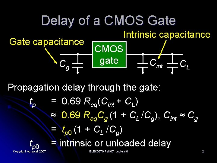
Delay of a CMOS Gate capacitance Cg Intrinsic capacitance CMOS gate Cint CL Propagation delay through the gate: tp = 0. 69 Req(Cint + CL) ≈ 0. 69 Req. Cg (1 + CL /Cg), Cint ≈ Cg = tp 0 (1 + CL /Cg) tp 0 = intrinsic or unloaded delay Copyright Agrawal, 2007 ELEC 6270 Fall 07, Lecture 6 2

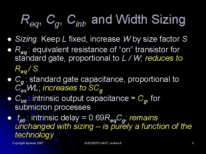
Req, Cg, Cint, and Width Sizing l l l Sizing: Keep L fixed, increase W by size factor S Req : equivalent resistance of “on” transistor for standard gate, proportional to L / W; reduces to Req / S Cg : standard gate capacitance, proportional to Cox. WL; increases to SCg Cint : intrinsic output capacitance ≈ Cg, for submicron processes tp 0 : intrinsic delay = 0. 69 Req. Cg; remains unchanged with sizing – is purely a function of the technology Copyright Agrawal, 2007 ELEC 6270 Fall 07, Lecture 6 3

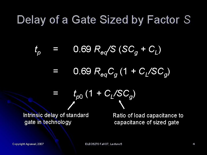
Delay of a Gate Sized by Factor S tp = 0. 69 Req/S (SCg + CL) = 0. 69 Req. Cg (1 + CL/SCg) = tp 0 (1 + CL/SCg) Intrinsic delay of standard gate in technology Copyright Agrawal, 2007 Ratio of load capacitance to capacitance of sized gate ELEC 6270 Fall 07, Lecture 6 4

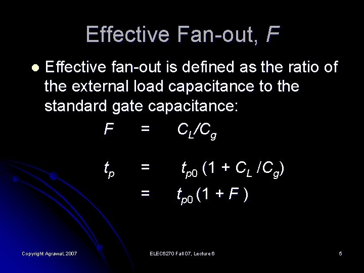
Effective Fan-out, F l Effective fan-out is defined as the ratio of the external load capacitance to the standard gate capacitance: F = CL/Cg tp Copyright Agrawal, 2007 = tp 0 (1 + CL /Cg) = tp 0 (1 + F ) ELEC 6270 Fall 07, Lecture 6 5

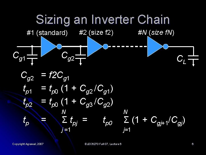
Sizing an Inverter Chain #1 (standard) Cg 1 #2 (size f 2) #N (size f. N) Cg 2 CL Cg 2 = f 2 Cg 1 tp 1 = tp 0 (1 + Cg 2 /Cg 1) tp 2 = tp 0 (1 + Cg 3 /Cg 2) tp = N Σ tpj = tp 0 j =1 Copyright Agrawal, 2007 N Σ (1 + Cgj+1/Cgj) j=1 ELEC 6270 Fall 07, Lecture 6 6

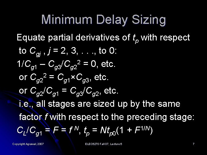
Minimum Delay Sizing Equate partial derivatives of tp with respect to Cgj , j = 2, 3, . . . , to 0: 1/Cg 1 – Cg 3/Cg 22 = 0, etc. or Cg 22 = Cg 1×Cg 3, etc. or Cg 2/Cg 1 = Cg 3/Cg 2, etc. i. e. , all stages are sized up by the same factor f with respect to the preceding stage: CL/Cg 1 = F = f N, tp = Ntp 0(1 + F 1/N) Copyright Agrawal, 2007 ELEC 6270 Fall 07, Lecture 6 7

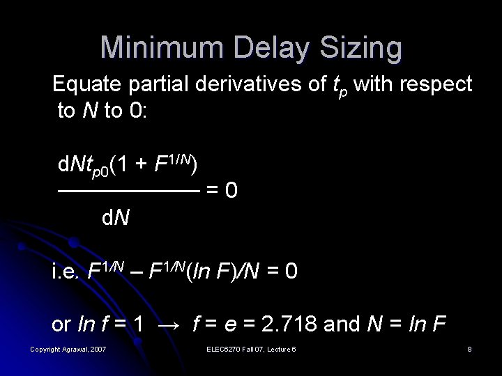
Minimum Delay Sizing Equate partial derivatives of tp with respect to N to 0: d. Ntp 0(1 + F 1/N) ───── = 0 d. N i. e. F 1/N – F 1/N(ln F)/N = 0 or ln f = 1 → f = e = 2. 718 and N = ln F Copyright Agrawal, 2007 ELEC 6270 Fall 07, Lecture 6 8

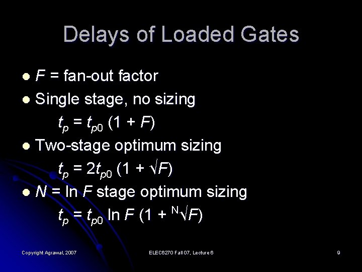
Delays of Loaded Gates F = fan-out factor l Single stage, no sizing tp = tp 0 (1 + F) l Two-stage optimum sizing tp = 2 tp 0 (1 + √F) l N = ln F stage optimum sizing tp = tp 0 ln F (1 + N√F) l Copyright Agrawal, 2007 ELEC 6270 Fall 07, Lecture 6 9

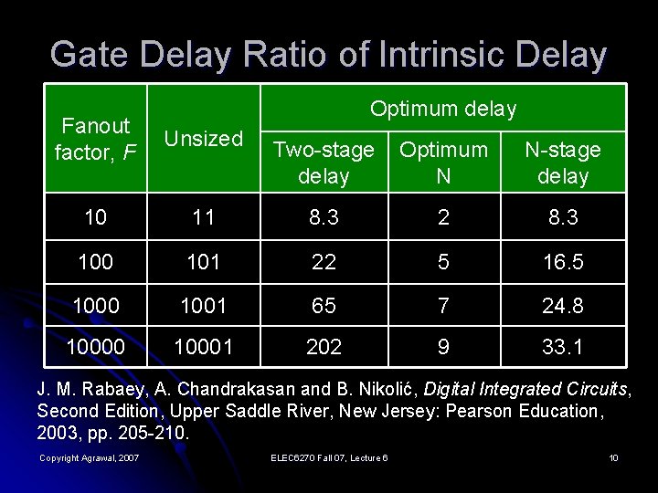
Gate Delay Ratio of Intrinsic Delay Optimum delay Fanout factor, F Unsized Two-stage delay Optimum N N-stage delay 10 11 8. 3 2 8. 3 100 101 22 5 16. 5 1000 1001 65 7 24. 8 10000 10001 202 9 33. 1 J. M. Rabaey, A. Chandrakasan and B. Nikolić, Digital Integrated Circuits, Second Edition, Upper Saddle River, New Jersey: Pearson Education, 2003, pp. 205 -210. Copyright Agrawal, 2007 ELEC 6270 Fall 07, Lecture 6 10

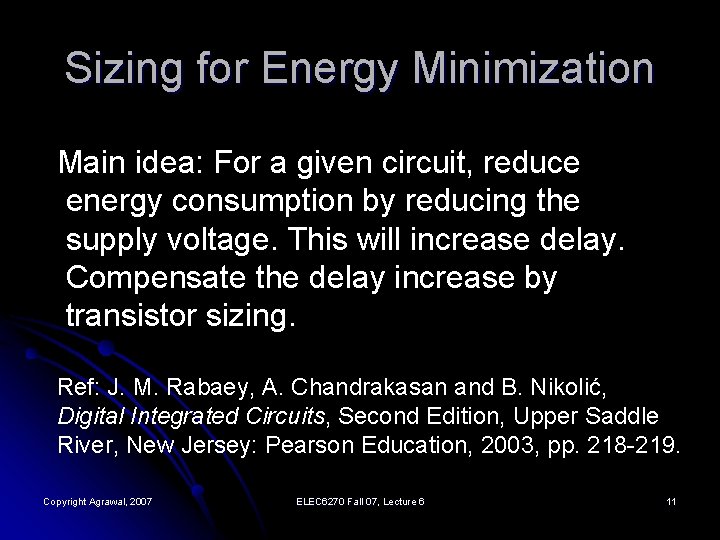
Sizing for Energy Minimization Main idea: For a given circuit, reduce energy consumption by reducing the supply voltage. This will increase delay. Compensate the delay increase by transistor sizing. Ref: J. M. Rabaey, A. Chandrakasan and B. Nikolić, Digital Integrated Circuits, Second Edition, Upper Saddle River, New Jersey: Pearson Education, 2003, pp. 218 -219. Copyright Agrawal, 2007 ELEC 6270 Fall 07, Lecture 6 11

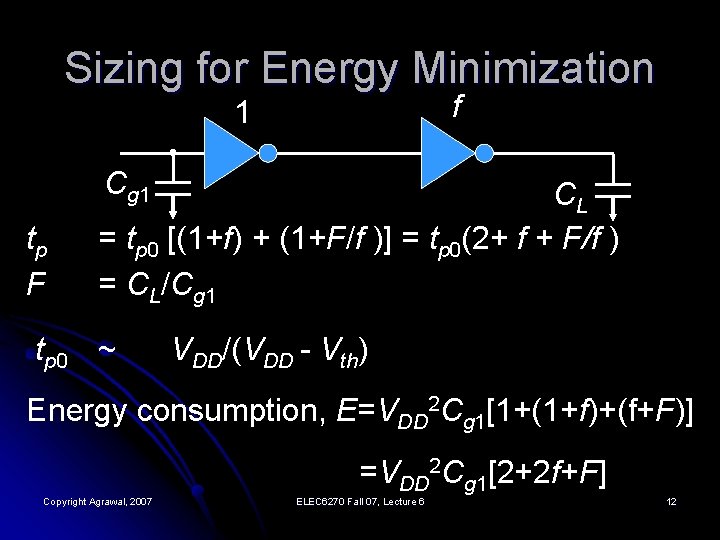
Sizing for Energy Minimization f 1 Cg 1 tp F CL = tp 0 [(1+f) + (1+F/f )] = tp 0(2+ f + F/f ) = CL/Cg 1 tp 0 ~ VDD/(VDD - Vth) Energy consumption, E=VDD 2 Cg 1[1+(1+f)+(f+F)] =VDD 2 Cg 1[2+2 f+F] Copyright Agrawal, 2007 ELEC 6270 Fall 07, Lecture 6 12

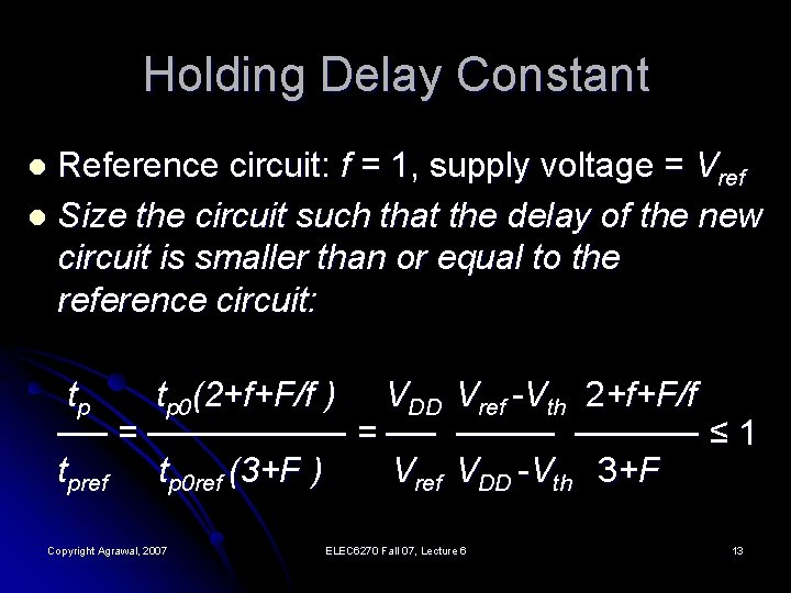
Holding Delay Constant Reference circuit: f = 1, supply voltage = Vref l Size the circuit such that the delay of the new circuit is smaller than or equal to the reference circuit: l tp tp 0(2+f+F/f ) VDD ── = ──── = ── tpref tp 0 ref (3+F ) Vref Copyright Agrawal, 2007 Vref -Vth 2+f+F/f ───── ≤ 1 VDD -Vth 3+F ELEC 6270 Fall 07, Lecture 6 13

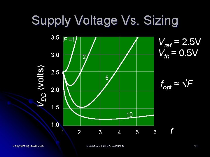
Supply Voltage Vs. Sizing 3. 5 F =1 VDD (volts) 3. 0 Vref = 2. 5 V Vth = 0. 5 V 2 2. 5 5 fopt ≈ √F 2. 0 1. 5 10 1. 0 1 Copyright Agrawal, 2007 2 3 4 ELEC 6270 Fall 07, Lecture 6 5 6 f 14

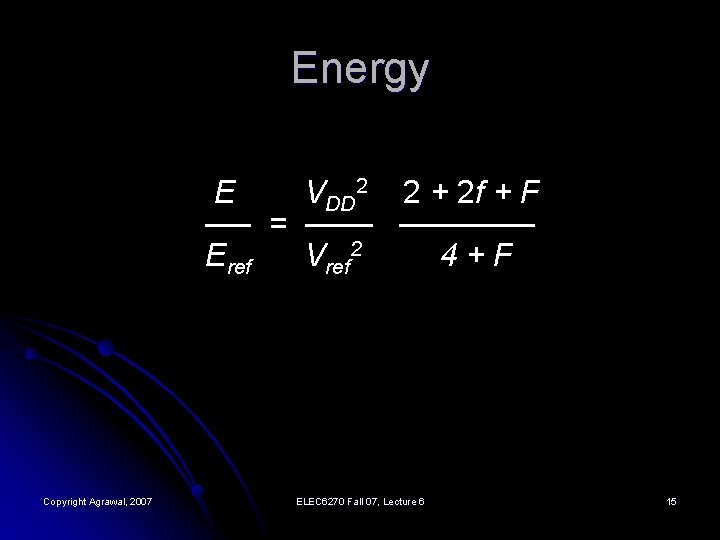
Energy E VDD 2 2 + 2 f + F ── = ────── Eref Vref 2 4+F Copyright Agrawal, 2007 ELEC 6270 Fall 07, Lecture 6 15

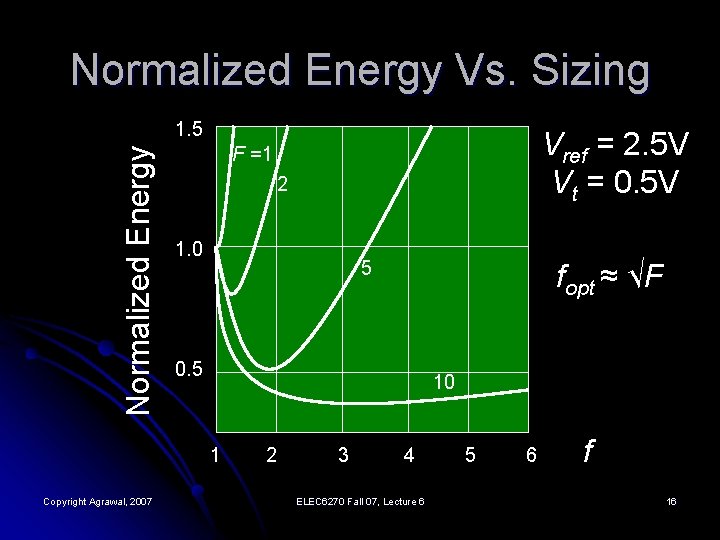
Normalized Energy Vs. Sizing Normalized Energy 1. 5 2 1. 0 5 fopt ≈ √F 0. 5 10 1 Copyright Agrawal, 2007 Vref = 2. 5 V Vt = 0. 5 V F =1 2 3 4 ELEC 6270 Fall 07, Lecture 6 5 6 f 16

Summary l l Device sizing combined with supply voltage reduction reduces energy consumption. For large fan-out energy reduction by a factor of 10 is possible. An exception is F = 1 case, where the minimum size device is also the most effective one. Oversizing the devices increases energy consumption. Copyright Agrawal, 2007 ELEC 6270 Fall 07, Lecture 6 17