ECE 3455 Electronics Chapter 3 Diodes Figures from

- Slides: 19

ECE 3455: Electronics Chapter 3: Diodes Figures from Sedra and Smith, Microelectronic Circuits 5 ed. , Oxford Press

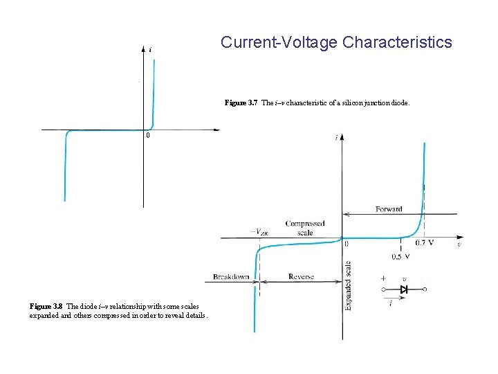
Current-Voltage Characteristics Figure 3. 7 The i–v characteristic of a silicon junction diode. Figure 3. 8 The diode i–v relationship with some scales expanded and others compressed in order to reveal details.

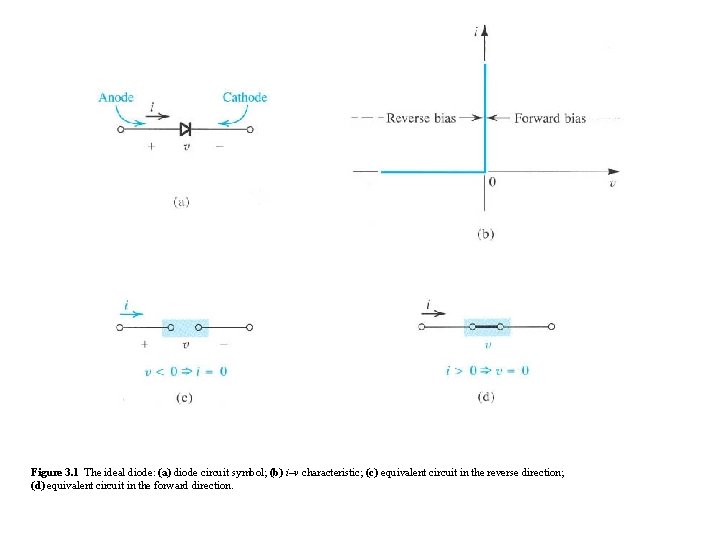
Figure 3. 1 The ideal diode: (a) diode circuit symbol; (b) i–v characteristic; (c) equivalent circuit in the reverse direction; (d) equivalent circuit in the forward direction.

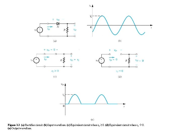
Figure 3. 3 (a) Rectifier circuit. (b) Input waveform. (c) Equivalent circuit when v. I 0. (d) Equivalent circuit when v. I 0. (e) Output waveform.

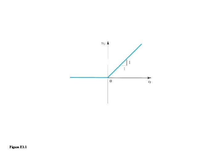
Figure E 3. 1

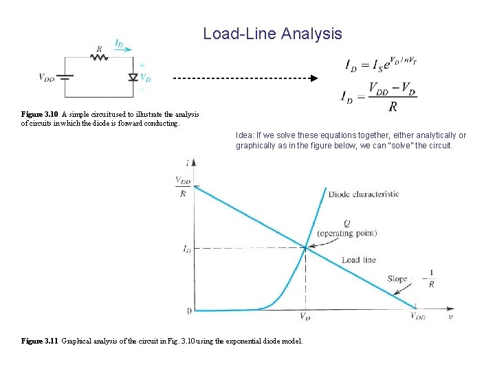
Load-Line Analysis Figure 3. 10 A simple circuit used to illustrate the analysis of circuits in which the diode is forward conducting. Idea: If we solve these equations together, either analytically or graphically as in the figure below, we can “solve” the circuit. Figure 3. 11 Graphical analysis of the circuit in Fig. 3. 10 using the exponential diode model.

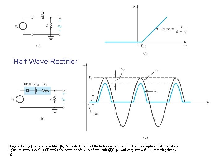
Half-Wave Rectifier Figure 3. 25 (a) Half-wave rectifier. (b) Equivalent circuit of the half-wave rectifier with the diode replaced with its battery -plus-resistance model. (c) Transfer characteristic of the rectifier circuit. (d) Input and output waveforms, assuming that r. D ! R.

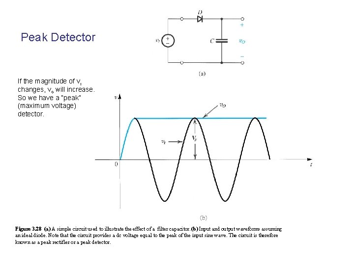
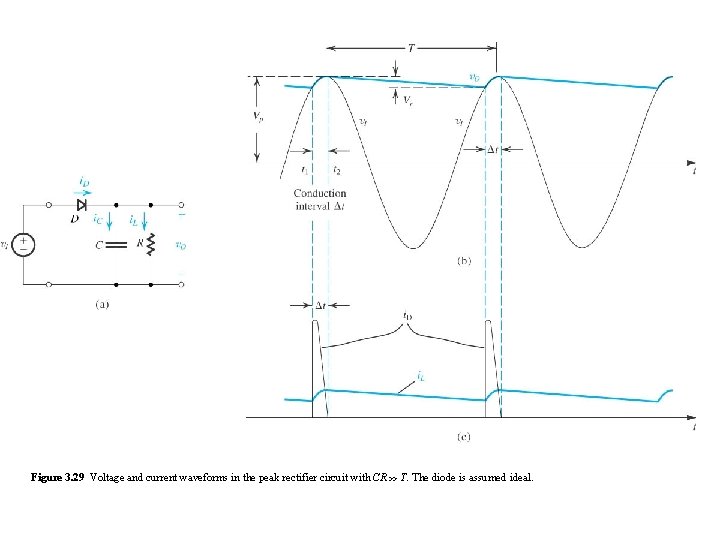
Peak Detector If the magnitude of vi changes, vo will increase. So we have a “peak” (maximum voltage) detector. Figure 3. 28 (a) A simple circuit used to illustrate the effect of a filter capacitor. (b) Input and output waveforms assuming an ideal diode. Note that the circuit provides a dc voltage equal to the peak of the input sine wave. The circuit is therefore known as a peak rectifier or a peak detector.

Figure 3. 29 Voltage and current waveforms in the peak rectifier circuit with CR >> T. The diode is assumed ideal.

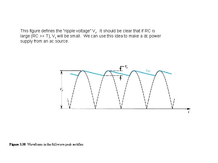
This figure defines the “ripple voltage” Vr. It should be clear that if RC is large (RC >> T), Vr will be small. We can use this idea to make a dc power supply from an ac source. Figure 3. 30 Waveforms in the full-wave peak rectifier.

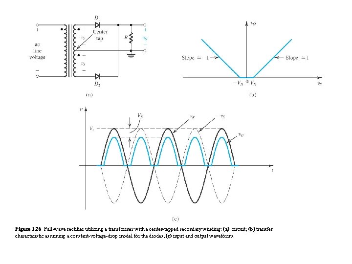
Figure 3. 26 Full-wave rectifier utilizing a transformer with a center-tapped secondary winding: (a) circuit; (b) transfer characteristic assuming a constant-voltage-drop model for the diodes; (c) input and output waveforms.

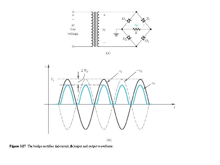
Figure 3. 27 The bridge rectifier: (a) circuit; (b) input and output waveforms.

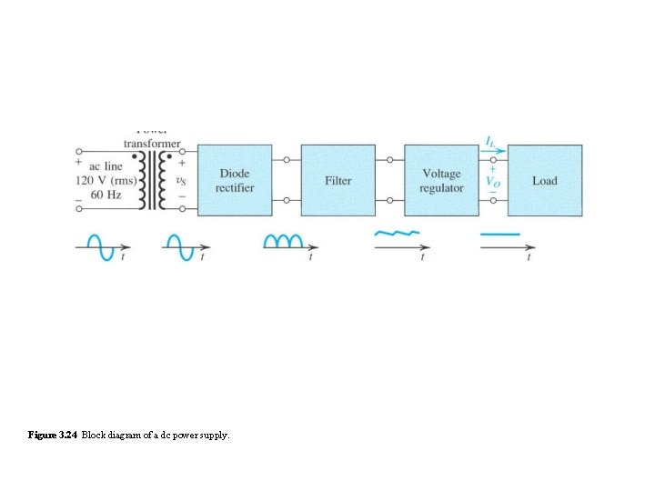
Figure 3. 24 Block diagram of a dc power supply.

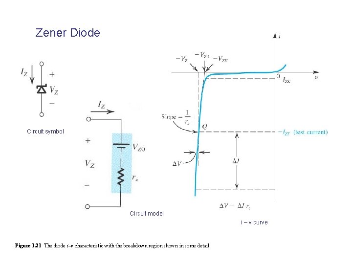
Zener Diode Circuit symbol Circuit model i – v curve Figure 3. 21 The diode i–v characteristic with the breakdown region shown in some detail.

Bistable Multivibrator Figure 13. 19 (a) The bistable circuit of Fig. 13. 17 with the negative input terminal of the op amp disconnected from ground and connected to an input signal v. I. (b) The transfer characteristic of the circuit in (a) for increasing v. I. (c) The transfer characteristic for decreasing v. I. (d) The complete transfer characteristics.

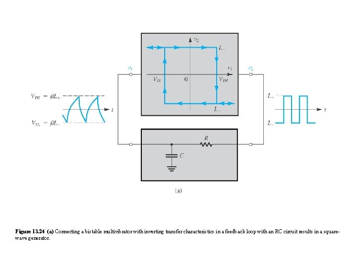
Figure 13. 24 (a) Connecting a bistable multivibrator with inverting transfer characteristics in a feedback loop with an RC circuit results in a squarewave generator.

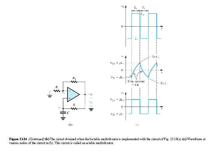
Figure 13. 24 (Continued) (b) The circuit obtained when the bistable multivibrator is implemented with the circuit of Fig. 13. 19(a). (c) Waveforms at various nodes of the circuit in (b). This circuit is called an astable multivibrator.

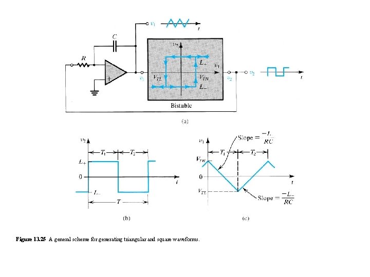
Figure 13. 25 A general scheme for generating triangular and square waveforms.

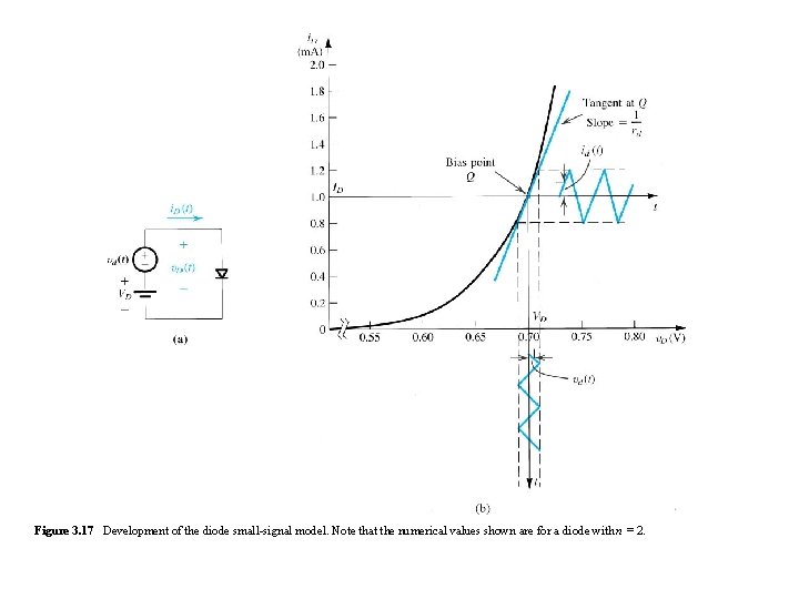
Figure 3. 17 Development of the diode small-signal model. Note that the numerical values shown are for a diode with n = 2.