Chapter 2 Diodes Electronics ECE 1312 Classification of
- Slides: 20

Chapter 2 Diodes © Electronics ECE 1312

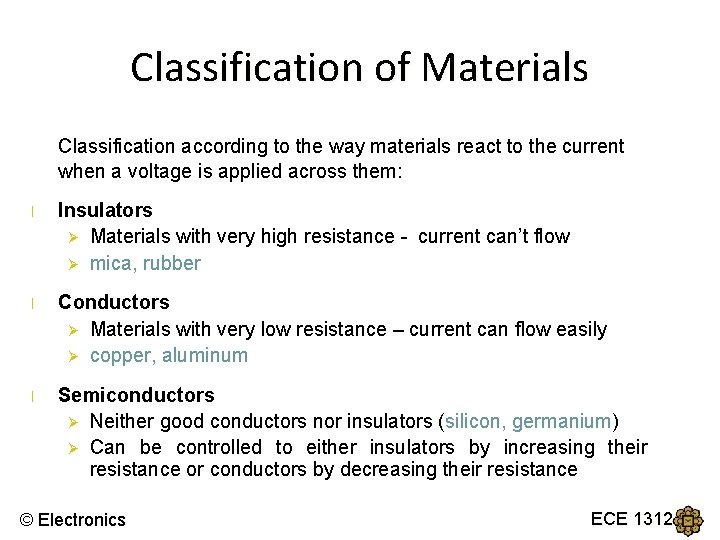
Classification of Materials Classification according to the way materials react to the current when a voltage is applied across them: l Insulators Ø Materials with very high resistance - current can’t flow Ø mica, rubber l Conductors Ø Materials with very low resistance – current can flow easily Ø copper, aluminum l Semiconductors Ø Neither good conductors nor insulators (silicon, germanium) Ø Can be controlled to either insulators by increasing their resistance or conductors by decreasing their resistance © Electronics ECE 1312

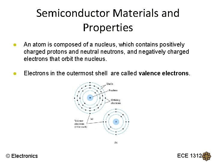
Semiconductor Materials and Properties ● An atom is composed of a nucleus, which contains positively charged protons and neutral neutrons, and negatively charged electrons that orbit the nucleus. ● Electrons in the outermost shell are called valence electrons. © Electronics ECE 1312

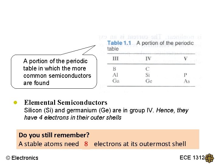
A portion of the periodic table in which the more common semiconductors are found ● Elemental Semiconductors Silicon (Si) and germanium (Ge) are in group IV. Hence, they have 4 electrons in their outer shells Do you still remember? A stable atoms need 8? electrons at its outermost shell © Electronics ECE 1312

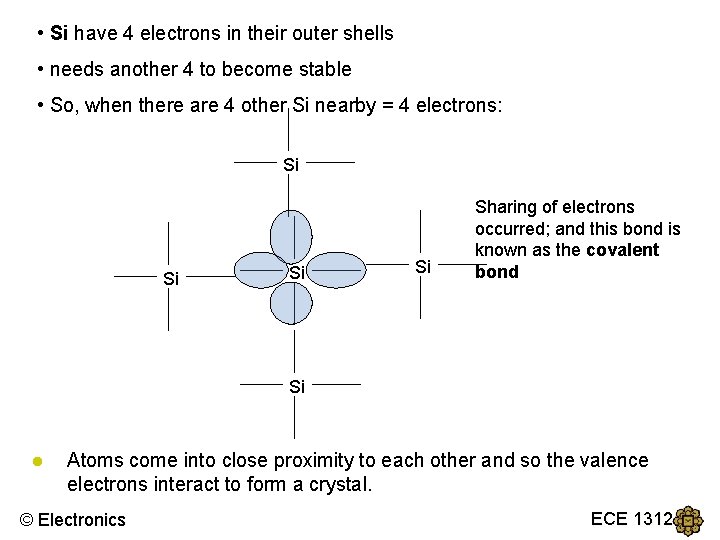
• Si have 4 electrons in their outer shells • needs another 4 to become stable • So, when there are 4 other Si nearby = 4 electrons: Si Si Sharing of electrons occurred; and this bond is known as the covalent bond Si ● Atoms come into close proximity to each other and so the valence electrons interact to form a crystal. © Electronics ECE 1312

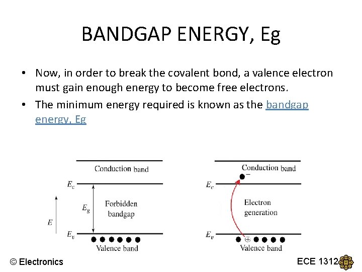
BANDGAP ENERGY, Eg • Now, in order to break the covalent bond, a valence electron must gain enough energy to become free electrons. • The minimum energy required is known as the bandgap energy, Eg © Electronics ECE 1312

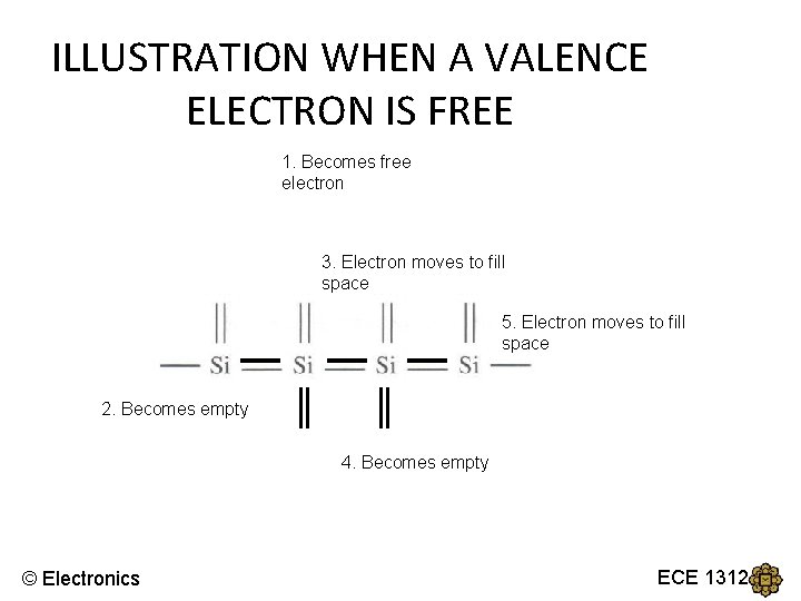
ILLUSTRATION WHEN A VALENCE ELECTRON IS FREE 1. Becomes free electron 3. Electron moves to fill space 5. Electron moves to fill space 2. Becomes empty 4. Becomes empty © Electronics ECE 1312

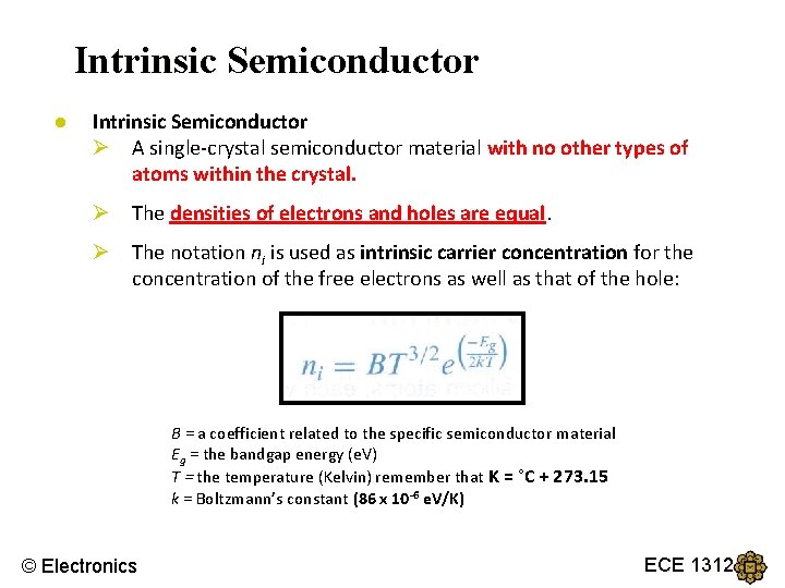
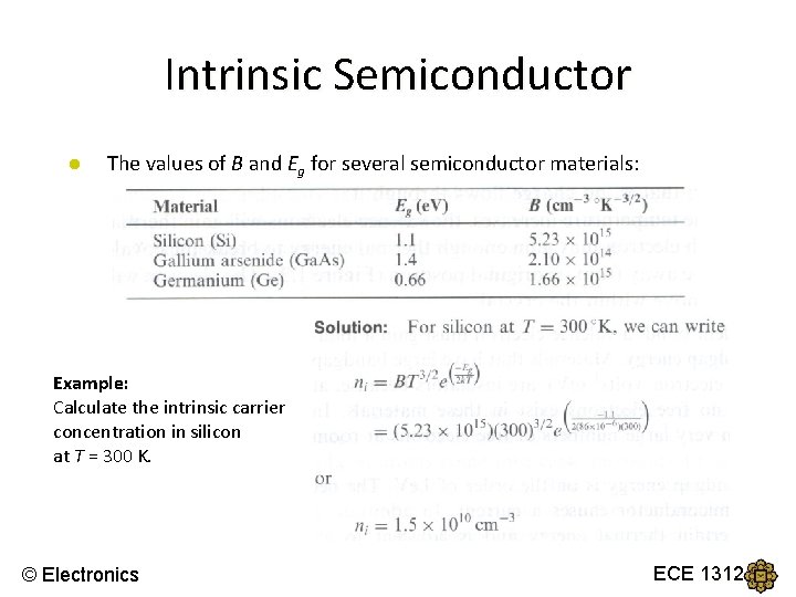
Intrinsic Semiconductor ● Intrinsic Semiconductor Ø A single-crystal semiconductor material with no other types of atoms within the crystal. Ø The densities of electrons and holes are equal. Ø The notation ni is used as intrinsic carrier concentration for the concentration of the free electrons as well as that of the hole: B = a coefficient related to the specific semiconductor material Eg = the bandgap energy (e. V) T = the temperature (Kelvin) remember that K = °C + 273. 15 k = Boltzmann’s constant (86 x 10 -6 e. V/K) © Electronics ECE 1312

Intrinsic Semiconductor ● The values of B and Eg for several semiconductor materials: Example: Calculate the intrinsic carrier concentration in silicon at T = 300 K. © Electronics ECE 1312

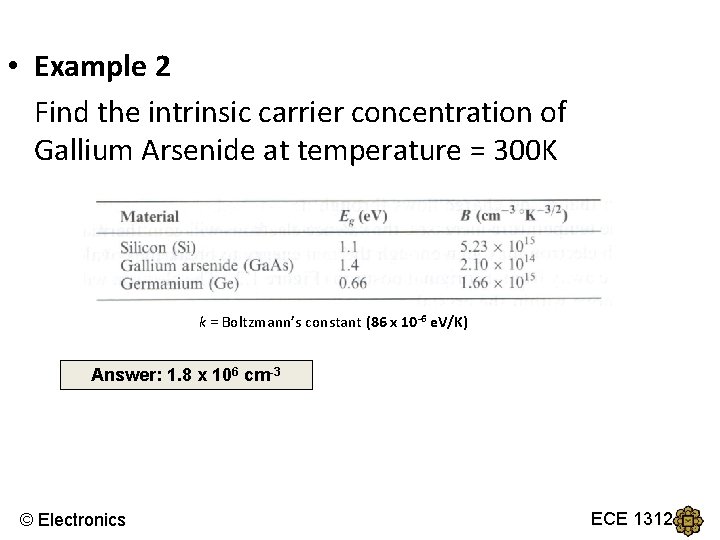
• Example 2 Find the intrinsic carrier concentration of Gallium Arsenide at temperature = 300 K k = Boltzmann’s constant (86 x 10 -6 e. V/K) Answer: 1. 8 x 106 cm-3 © Electronics ECE 1312

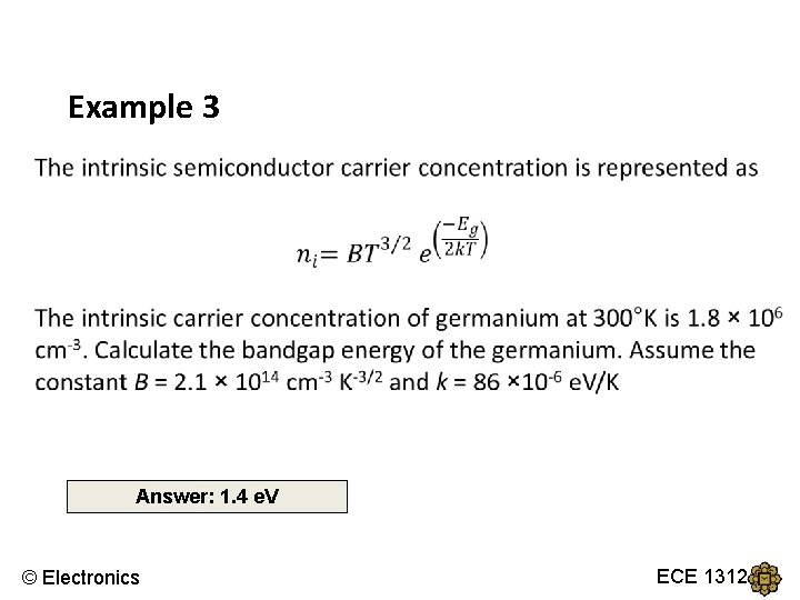
Example 3 Answer: 1. 4 e. V © Electronics ECE 1312

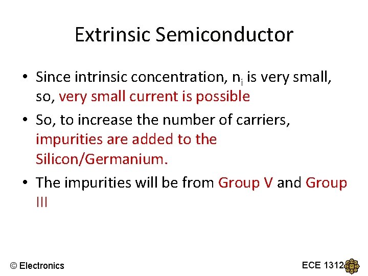
Extrinsic Semiconductor • Since intrinsic concentration, ni is very small, so, very small current is possible • So, to increase the number of carriers, impurities are added to the Silicon/Germanium. • The impurities will be from Group V and Group III © Electronics ECE 1312

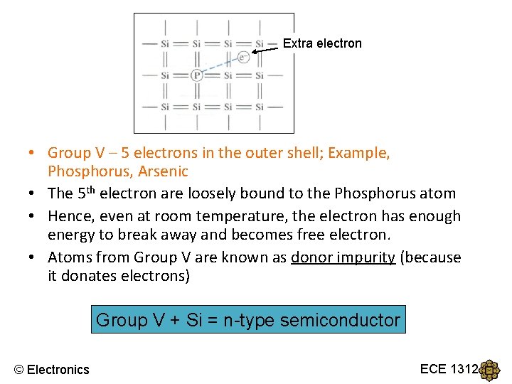
Extra electron • Group V – 5 electrons in the outer shell; Example, Phosphorus, Arsenic • The 5 th electron are loosely bound to the Phosphorus atom • Hence, even at room temperature, the electron has enough energy to break away and becomes free electron. • Atoms from Group V are known as donor impurity (because it donates electrons) Group V + Si = n-type semiconductor © Electronics ECE 1312

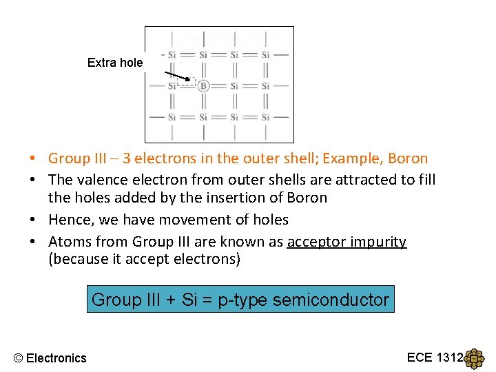
Extra hole • Group III – 3 electrons in the outer shell; Example, Boron • The valence electron from outer shells are attracted to fill the holes added by the insertion of Boron • Hence, we have movement of holes • Atoms from Group III are known as acceptor impurity (because it accept electrons) Group III + Si = p-type semiconductor © Electronics ECE 1312

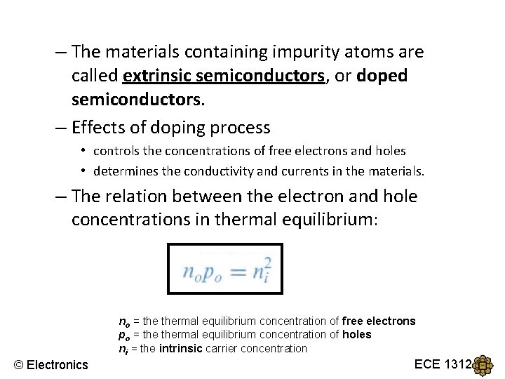
– The materials containing impurity atoms are called extrinsic semiconductors, or doped semiconductors. – Effects of doping process • controls the concentrations of free electrons and holes • determines the conductivity and currents in the materials. – The relation between the electron and hole concentrations in thermal equilibrium: no = thermal equilibrium concentration of free electrons po = thermal equilibrium concentration of holes ni = the intrinsic carrier concentration © Electronics ECE 1312

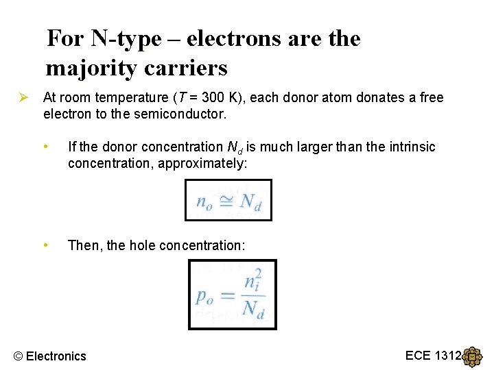
For N-type – electrons are the majority carriers Ø At room temperature (T = 300 K), each donor atom donates a free electron to the semiconductor. • If the donor concentration Nd is much larger than the intrinsic concentration, approximately: • Then, the hole concentration: © Electronics ECE 1312

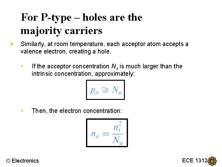
For P-type – holes are the majority carriers Ø Similarly, at room temperature, each acceptor atom accepts a valence electron, creating a hole. • If the acceptor concentration Na is much larger than the intrinsic concentration, approximately: • Then, the electron concentration: © Electronics ECE 1312

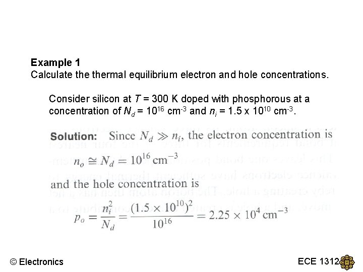
Example 1 Calculate thermal equilibrium electron and hole concentrations. Consider silicon at T = 300 K doped with phosphorous at a concentration of Nd = 1016 cm-3 and ni = 1. 5 x 1010 cm-3. © Electronics ECE 1312

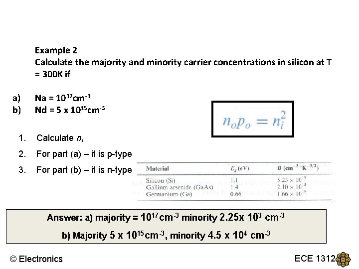
Example 2 Calculate the majority and minority carrier concentrations in silicon at T = 300 K if a) b) Na = 1017 cm-3 Nd = 5 x 1015 cm-3 1. Calculate ni 2. For part (a) – it is p-type 3. For part (b) – it is n-type Answer: a) majority = 1017 cm-3 minority 2. 25 x 103 cm-3 b) Majority 5 x 1015 cm-3, minority 4. 5 x 104 cm-3 © Electronics ECE 1312

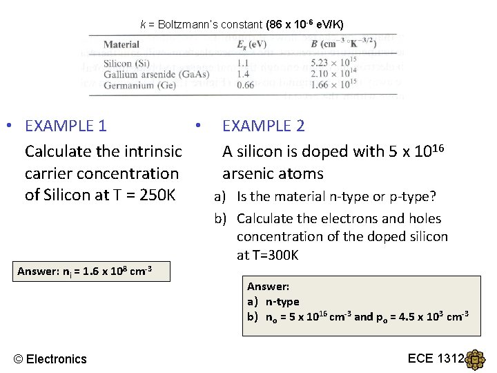
k = Boltzmann’s constant (86 x 10 -6 e. V/K) • EXAMPLE 1 • EXAMPLE 2 Calculate the intrinsic A silicon is doped with 5 x 10¹⁶ carrier concentration arsenic atoms of Silicon at T = 250 K a) Is the material n-type or p-type? Answer: ni = 1. 6 x 108 cm-3 © Electronics b) Calculate the electrons and holes concentration of the doped silicon at T=300 K Answer: a) n-type b) no = 5 x 1016 cm-3 and po = 4. 5 x 103 cm-3 ECE 1312