Digital Electronics Principles Applications Fifth Edition Roger L
- Slides: 18

Digital Electronics Principles & Applications Fifth Edition Roger L. Tokheim Chapter 5 IC Specifications and Simple Interfacing © 1999 Glencoe/Mc. Graw-Hill

CHAPTER 5 PREVIEW • Logic Levels/Noise Margin • Other Specifications • MOS and CMOS ICs • Interfacing with Switches • Interfacing with LEDs • Interfacing ICs • Interfacing with Buzzers, Relays, Motors and Solenoids • Optoisolators • Interfacing with Stepper Motors

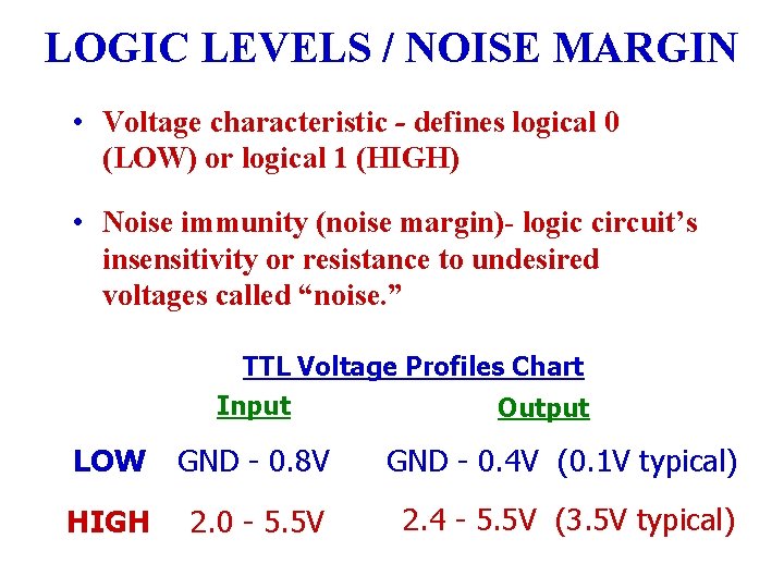
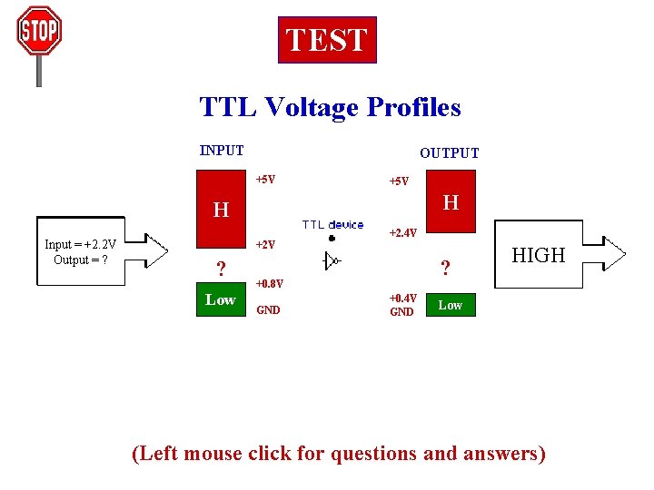
LOGIC LEVELS / NOISE MARGIN • Voltage characteristic - defines logical 0 (LOW) or logical 1 (HIGH) • Noise immunity (noise margin)- logic circuit’s insensitivity or resistance to undesired voltages called “noise. ” TTL Voltage Profiles Chart Input Output LOW GND - 0. 8 V GND - 0. 4 V (0. 1 V typical) HIGH 2. 0 - 5. 5 V 2. 4 - 5. 5 V (3. 5 V typical)

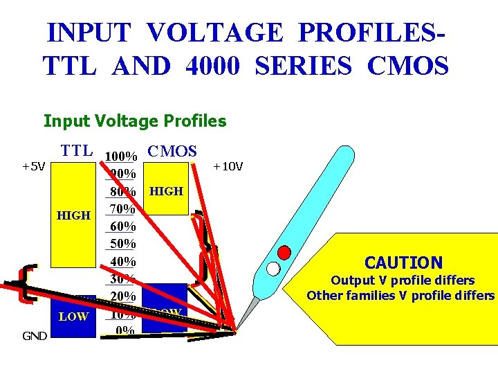
INPUT VOLTAGE PROFILESTTL AND 4000 SERIES CMOS Input Voltage Profiles +5 V TTL 100% CMOS HIGH LOW GND 90% 80% HIGH 70% 60% 50% 40% 30% 20% 10% LOW 0% +10 V CAUTION LOW Undefined Output. Undefined V profile differs HIGH logic reading may 0+3 toprobe +3 V for CMOS Other families profile to +7 VVfor CMOSdiffers depending on +7 V +10 V - for CMOS 0 vary tototo +0. 8 V TTL +0. 8 V +2. 0 Vin TTL manufacturer +2 V to +5 V - TTL

TEST TTL Voltage Profiles INPUT OUTPUT +5 V H H Input +1. 2 V Input==+0. 3 V +4 V +2. 2 V Output = ? +2 V ? Low +2. 4 V ? +0. 8 V GND +0. 4 V GND Undefined ? HIGH LOW Low (Left mouse click for questions and answers)

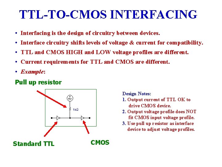
TTL-TO-CMOS INTERFACING • Interfacing is the design of circuitry between devices. • Interface circuitry shifts levels of voltage & current for compatibility. • TTL and CMOS HIGH and LOW voltage profiles are different. • Current requirements for TTL and CMOS are different. • Example: Pull up resistor Design Notes: 1. Output current of TTL OK to drive CMOS device. 2. Output voltage profile does NOT fit CMOS input voltage profile. 3. Use pull up resistor as interface device to adjust voltage profiles. Standard TTL CMOS

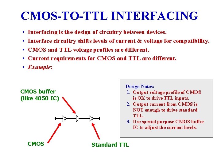
CMOS-TO-TTL INTERFACING • • • Interfacing is the design of circuitry between devices. Interface circuitry shifts levels of current & voltage for compatibility. CMOS and TTL voltage profiles are different. Current requirements for CMOS and TTL are different. Example: CMOS buffer (like 4050 IC) CMOS Design Notes: 1. Output voltage profile of CMOS is OK to drive TTL inputs. 2. Output current from CMOS is NOT enough to drive standard TTL. 3. Use special purpose CMOS buffer IC to adjust the current levels. Standard TTL

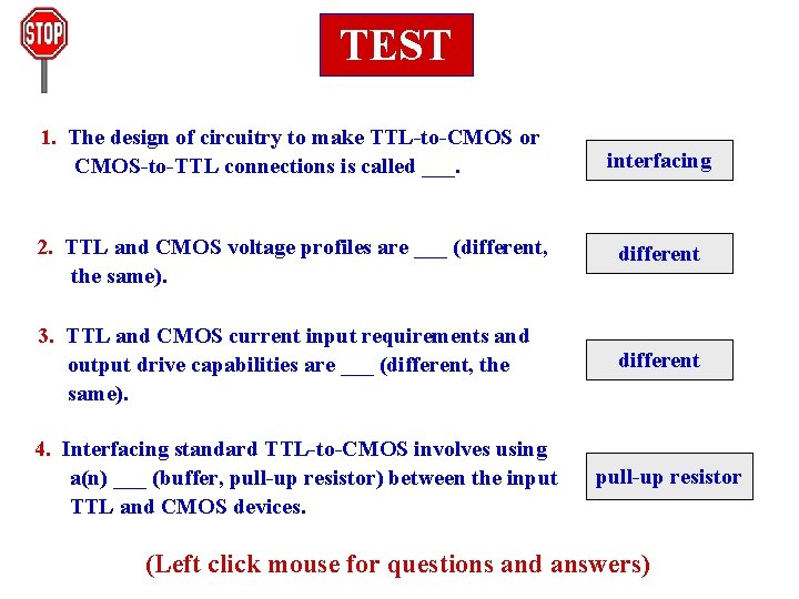
TEST 1. The design of circuitry to make TTL-to-CMOS or CMOS-to-TTL connections is called ___. interfacing 2. TTL and CMOS voltage profiles are ___ (different, the same). different 3. TTL and CMOS current input requirements and output drive capabilities are ___ (different, the same). different 4. Interfacing standard TTL-to-CMOS involves using a(n) ___ (buffer, pull-up resistor) between the input TTL and CMOS devices. pull-up resistor (Left click mouse for questions and answers)

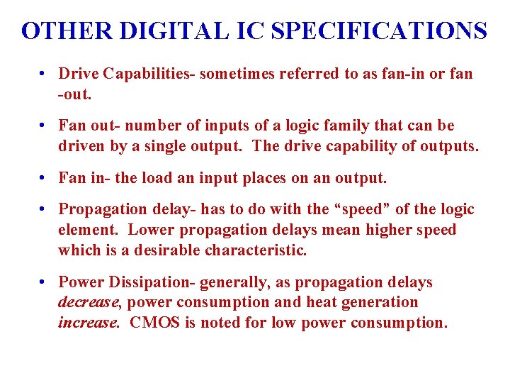
OTHER DIGITAL IC SPECIFICATIONS • Drive Capabilities- sometimes referred to as fan-in or fan -out. • Fan out- number of inputs of a logic family that can be driven by a single output. The drive capability of outputs. • Fan in- the load an input places on an output. • Propagation delay- has to do with the “speed” of the logic element. Lower propagation delays mean higher speed which is a desirable characteristic. • Power Dissipation- generally, as propagation delays decrease, power consumption and heat generation increase. CMOS is noted for low power consumption.

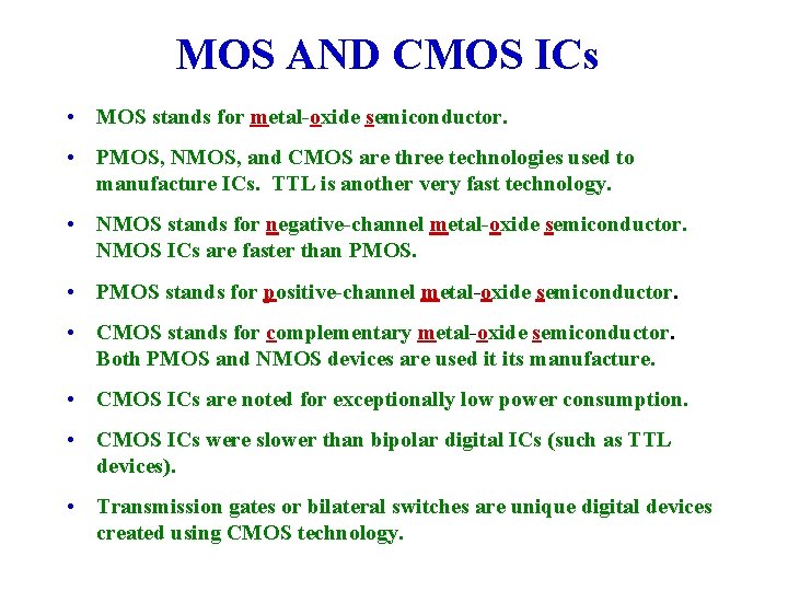
MOS AND CMOS ICs • MOS stands for metal-oxide semiconductor. • PMOS, NMOS, and CMOS are three technologies used to manufacture ICs. TTL is another very fast technology. • NMOS stands for negative-channel metal-oxide semiconductor. NMOS ICs are faster than PMOS. • PMOS stands for positive-channel metal-oxide semiconductor. • CMOS stands for complementary metal-oxide semiconductor. Both PMOS and NMOS devices are used it its manufacture. • CMOS ICs are noted for exceptionally low power consumption. • CMOS ICs were slower than bipolar digital ICs (such as TTL devices). • Transmission gates or bilateral switches are unique digital devices created using CMOS technology.

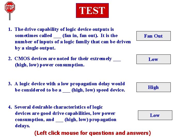
TEST 1. The drive capability of logic device outputs is sometimes called ___ (fan in, fan out). It is the number of inputs of a logic family that can be driven by a single output. Fan Out 2. CMOS devices are noted for their extremely ___ (high, low) power consumption. Low 3. A logic device with a low propagation delay would be considered to be a ___ (high, low) speed device. High 4. Several desirable characteristics of logic devices are good drive capabilities, low power Low consumption, and ___ (high, low) propagation delays. (Left click mouse for questions and answers)

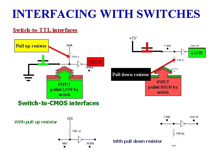
INTERFACING WITH SWITCHES Switch-to-TTL interfaces +5 V Pull up resistor HIGH LOW INPUT pulled HIGH by pulled LOW by pull up resistor pulled LOW by pull switch up resistor switch Pull down resistor INPUT pulled LOW by by pulled HIGH by pull down resistor switch Switch-to-CMOS interfaces With pull up resistor With pull down resistor

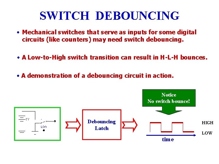
SWITCH DEBOUNCING • Mechanical switches that serve as inputs for some digital circuits (like counters) may need switch debouncing. • A Low-to-High switch transition can result in H-L-H bounces. • A demonstration of a debouncing circuit in action. Notice No switch bounce! Debouncing Latch HIGH LOW time

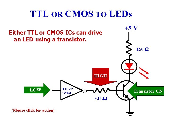
TTL OR CMOS TO LEDs Either TTL or CMOS ICs can drive an LED using a transistor. +5 V 150 W HIGH LOW HIGH TTL or CMOS Transistor Off ON 33 k. W (Mouse click for action)

INTERFACING WITH BUZZERS, RELAYS, MOTORS & SOLENOIDS • Piezo buzzer - a signaling device drawing less current than older buzzers and bells. • DC or AC motors - produce continuous rotary motion. (Motor voltages and current not compatible with logic circuits. ) • Solenoid - a device that can produce linear motion. • Relay - a device to isolate logic device from highvoltage/current circuit. • Optoisolator - a device to isolate logic device from highvoltage/current circuit.

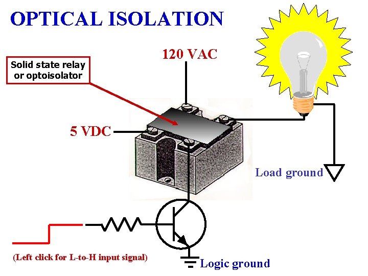
ISOLATION- LOGIC TO HIGH VOLTAGE/CURRENT • Electromechanical relays - older method of isolation. Relays are expensive, heavy, and produce “noise. ” • Optoisolator (optocoupler) - light weight alternative to electromagnetic relay when interfacing with logic circuits. • Solid state relay - a heavy-duty version of an optoisolator.

OPTICAL ISOLATION Solid state relay or optoisolator 120 VAC 5 VDC Load ground (Left click for L-to-H input signal) Logic ground

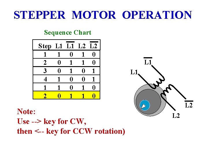
STEPPER MOTOR OPERATION Sequence Chart Step 1 2 3 4 1 2 L 1 1 0 0 1 1 0 L 1 L 2 0 1 1 0 1 0 1 1 0 Note: Use --> key for CW, then <-- key for CCW rotation) L 1 L 2