CPU 08 INTRODUCTION Motorola CPU 08 Core Execution


- Slides: 14
CPU 08 INTRODUCTION Motorola CPU 08 Core Execution Architecture MTT 48 3 -1
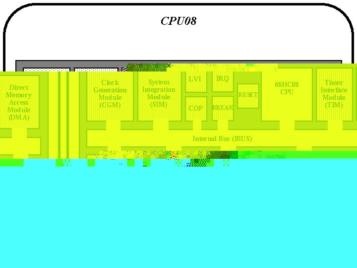
CPU 08 Clock Generation Module (CGM) System Integration Module (SIM) LVI IRQ RESET COP 68 HC 08 CPU BREAK Timer Interface Module (TIM) Direct Memory Access Module (DMA) Internal Bus (IBUS) Serial Communications Interface (SCI) Motorola Serial Peripheral Interface (SPI) Random Access Memory (RAM) Electronically Programmable Memory (EPROM) Monitor ROM CPU 08 Core Execution Architecture MTT 48 3 -2
Module Exercise Objectives At end of sections coming up, will write • Subroutine that clears all RAM locations • Code sequence that executes at Power-on or RESET and calls the RAM clearing subroutine Motorola CPU 08 Core Execution Architecture MTT 48 3 -3
CPU 08 EXECUTION ARCHITECTURE Motorola CPU 08 Core Execution Architecture MTT 48 3 -4
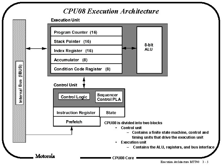
CPU 08 Execution Architecture CPU 08 is divided into two blocks • Control unit – Contains a finite state machine, control and timing units that drive the execution unit • Execution unit – Contains the ALU, registers, and bus interface Motorola CPU 08 Core Execution Architecture MTT 48 3 -5
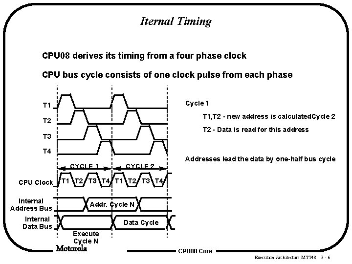
Iternal Timing CPU 08 derives its timing from a four phase clock CPU bus cycle consists of one clock pulse from each phase Cycle 1 T 1, T 2 - new address is calculated. Cycle 2 T 2 - Data is read for this address T 3 T 4 CYCLE 1 CPU Clock T 1 T 2 T 3 T 4 Internal Address Bus Internal Data Bus CYCLE 2 Addresses lead the data by one-half bus cycle Addr. Cycle N Data Cycle Execute Cycle N Motorola CPU 08 Core Execution Architecture MTT 48 3 -6
CPU 08 Prefetch HC 05 has many cycles where the address and data bus are idle CPU 08 contains an opcode "look ahead" prefetch mechanism • Performance increases were achieved by removing as many dead bus cycles as possible. CPU 08 instruction flow was developed to be as efficient as possible in a pipelined architecture Motorola CPU 08 Core Execution Architecture MTT 48 3 -7
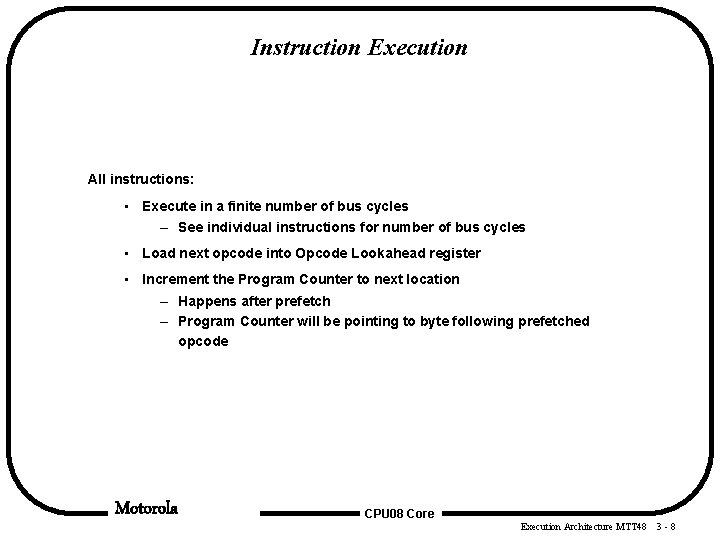
Instruction Execution All instructions: • Execute in a finite number of bus cycles – See individual instructions for number of bus cycles • Load next opcode into Opcode Lookahead register • Increment the Program Counter to next location – Happens after prefetch – Program Counter will be pointing to byte following prefetched opcode Motorola CPU 08 Core Execution Architecture MTT 48 3 -8
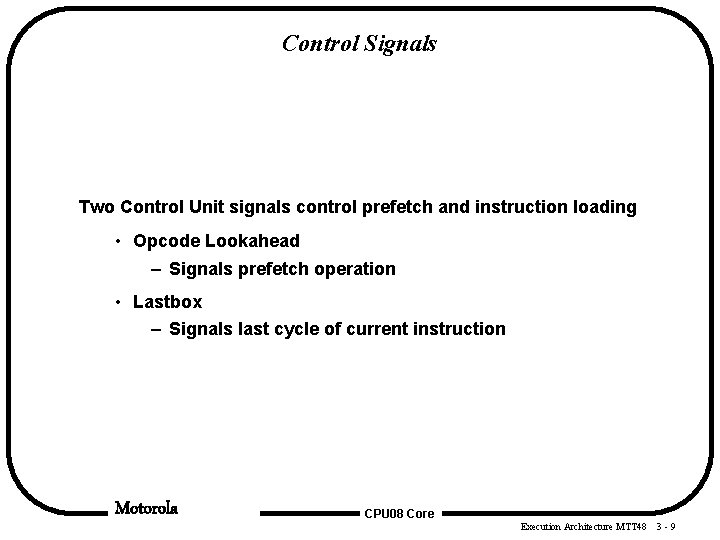
Control Signals Two Control Unit signals control prefetch and instruction loading • Opcode Lookahead – Signals prefetch operation • Lastbox – Signals last cycle of current instruction Motorola CPU 08 Core Execution Architecture MTT 48 3 -9
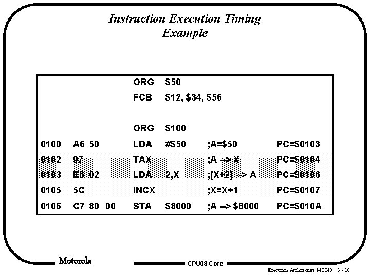
Instruction Execution Timing Example ORG $50 FCB $12, $34, $56 ORG $100 #$50 0100 A 6 50 LDA 0102 97 TAX 0103 E 6 02 LDA 0105 5 C INCX 0106 C 7 80 00 STA Motorola 2, X $8000 ; A=$50 PC=$0103 ; A --> X PC=$0104 ; [X+2] --> A PC=$0106 ; X=X+1 PC=$0107 ; A --> $8000 PC=$010 A CPU 08 Core Execution Architecture MTT 48 3 - 10
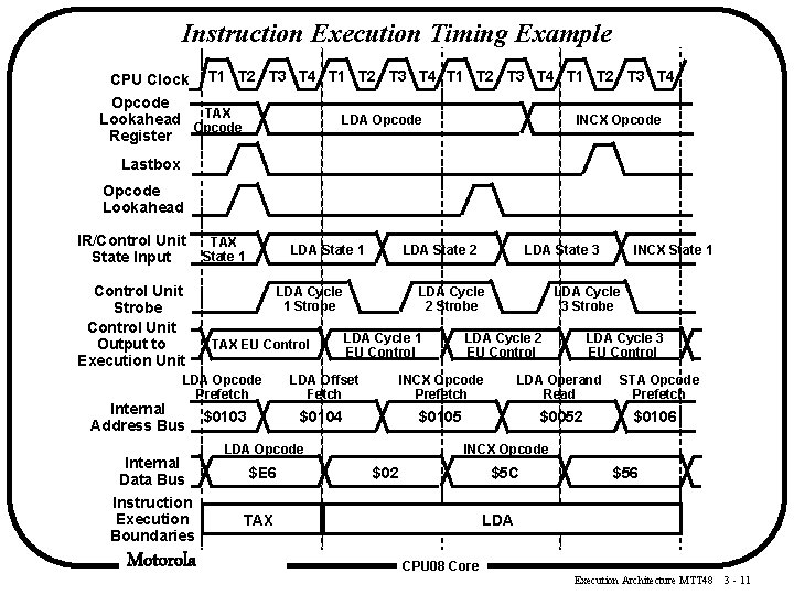
Instruction Execution Timing Example CPU Clock T 1 T 2 T 3 T 4 Opcode TAX LDA Opcode INCX Opcode Lookahead Opcode Register Lastbox Opcode Lookahead IR/Control Unit State Input Control Unit Strobe Control Unit Output to Execution Unit TAX State 1 LDA State 2 LDA Cycle 1 Strobe TAX EU Control LDA State 3 LDA Cycle 2 Strobe LDA Cycle 1 EU Control LDA Cycle 3 Strobe LDA Cycle 2 EU Control LDA Cycle 3 EU Control LDA Opcode Prefetch LDA Offset Fetch INCX Opcode Prefetch LDA Operand Read $0103 $0104 $0105 $0052 Internal Address Bus Internal Data Bus Instruction Execution Boundaries Motorola LDA Opcode $E 6 INCX State 1 STA Opcode Prefetch $0106 INCX Opcode $02 $5 C TAX $56 LDA CPU 08 Core Execution Architecture MTT 48 3 - 11
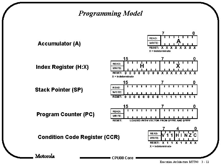
Programming Model Accumulator (A) Index Register (H: X) Stack Pointer (SP) Program Counter (PC) Condition Code Register (CCR) Motorola CPU 08 Core Execution Architecture MTT 48 3 - 12
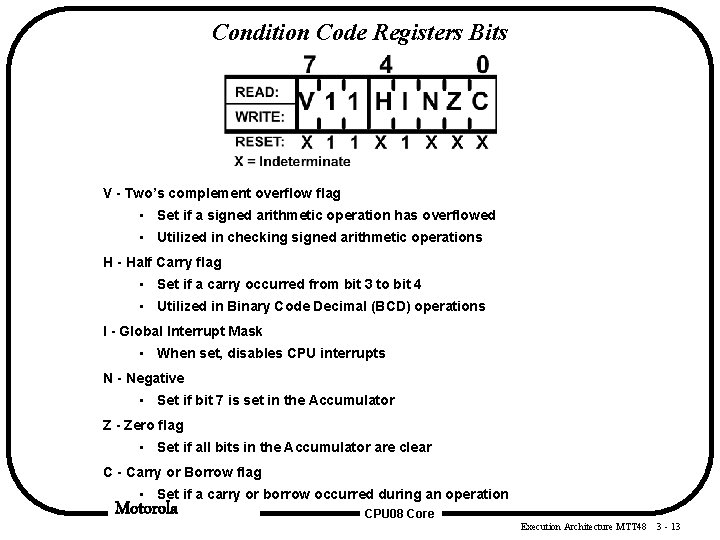
Condition Code Registers Bits V - Two’s complement overflow flag • Set if a signed arithmetic operation has overflowed • Utilized in checking signed arithmetic operations H - Half Carry flag • Set if a carry occurred from bit 3 to bit 4 • Utilized in Binary Code Decimal (BCD) operations I - Global Interrupt Mask • When set, disables CPU interrupts N - Negative • Set if bit 7 is set in the Accumulator Z - Zero flag • Set if all bits in the Accumulator are clear C - Carry or Borrow flag • Set if a carry or borrow occurred during an operation Motorola CPU 08 Core Execution Architecture MTT 48 3 - 13
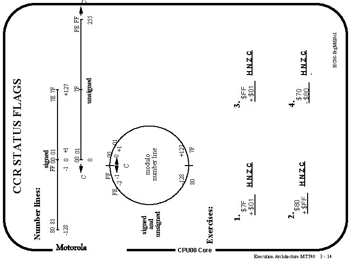
signed and unsigned $80 + $FF 2. $7 F + $01 1. C 00 0 +1 01 7 F 80 HNZC +127 -128 modulo number line FF FE -2 -1 0 $70 - $80 4. $FF + $01 3. unsigned 7 F 00 01 C +127 -1 0 +1 -128 7 E 7 F FF 00 01 80 81 signed CCR STATUS FLAGS Number lines: Exercises: Motorola CPU 08 Core Execution Architecture MTT 48 3 - 14 HC 08 -Prg. Mdl. Sol HNZC - HNZC 255 FE FF C