Chapter 13 DMA Programming 1 DMA Usage of

- Slides: 17

Chapter 13 DMA Programming 1

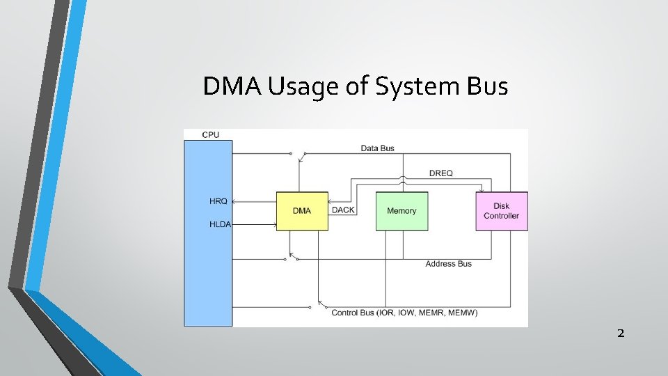
DMA Usage of System Bus 2

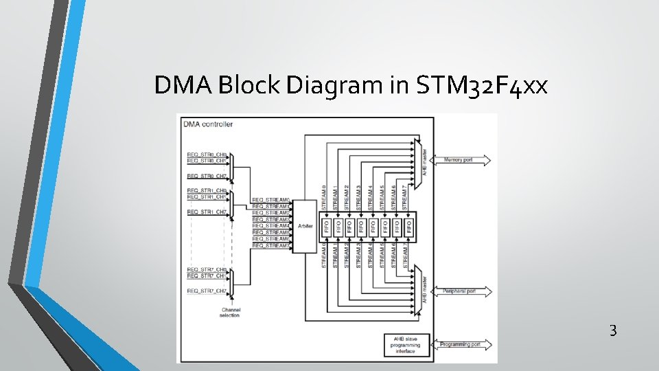
DMA Block Diagram in STM 32 F 4 xx 3

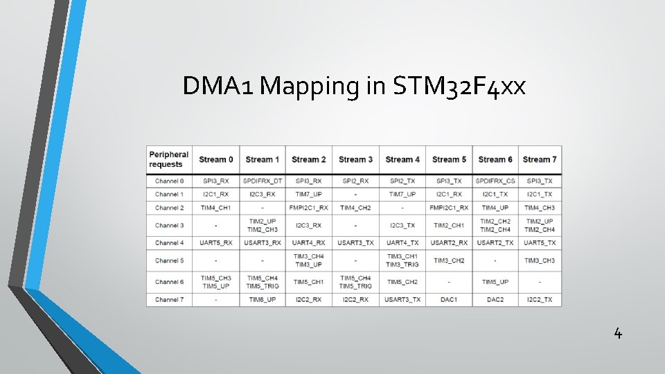
DMA 1 Mapping in STM 32 F 4 xx 4

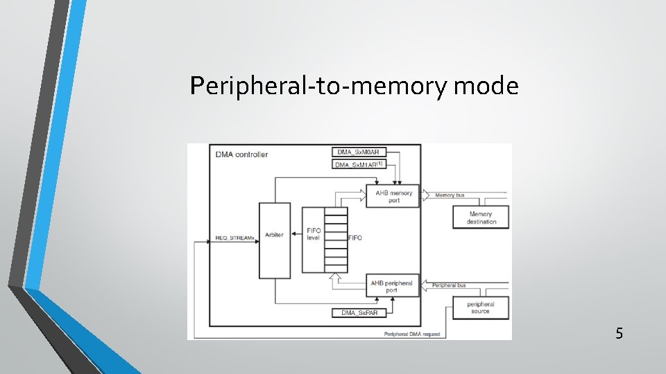
Peripheral-to-memory mode 5

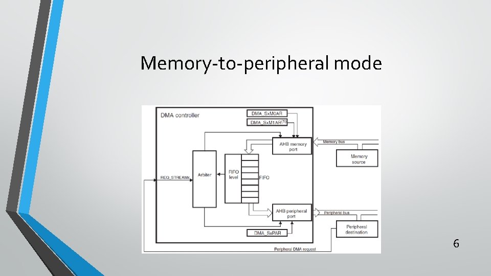
Memory-to-peripheral mode 6

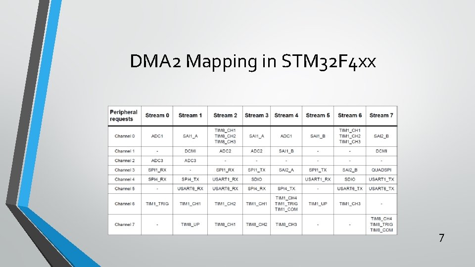
DMA 2 Mapping in STM 32 F 4 xx 7

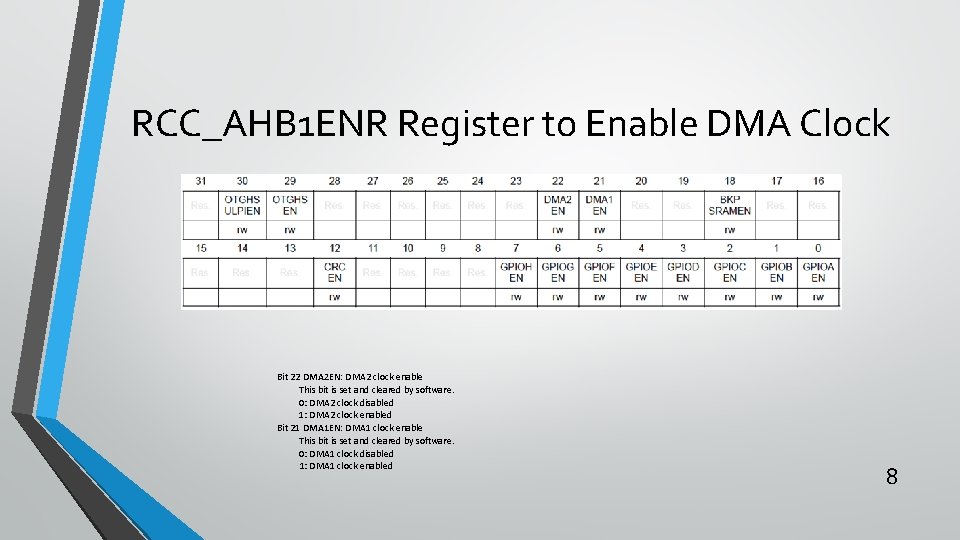
RCC_AHB 1 ENR Register to Enable DMA Clock Bit 22 DMA 2 EN: DMA 2 clock enable This bit is set and cleared by software. 0: DMA 2 clock disabled 1: DMA 2 clock enabled Bit 21 DMA 1 EN: DMA 1 clock enable This bit is set and cleared by software. 0: DMA 1 clock disabled 1: DMA 1 clock enabled 8

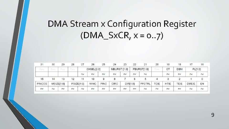
DMA Stream x Configuration Register (DMA_Sx. CR, x = 0. . 7) 9

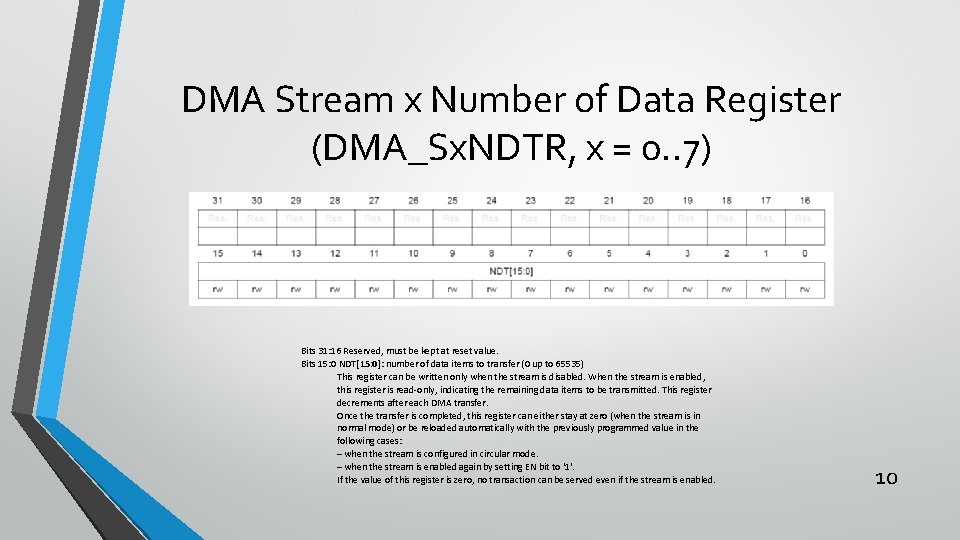
DMA Stream x Number of Data Register (DMA_Sx. NDTR, x = 0. . 7) Bits 31: 16 Reserved, must be kept at reset value. Bits 15: 0 NDT[15: 0]: number of data items to transfer (0 up to 65535) This register can be written only when the stream is disabled. When the stream is enabled, this register is read-only, indicating the remaining data items to be transmitted. This register decrements after each DMA transfer. Once the transfer is completed, this register can either stay at zero (when the stream is in normal mode) or be reloaded automatically with the previously programmed value in the following cases: – when the stream is configured in circular mode. – when the stream is enabled again by setting EN bit to '1'. If the value of this register is zero, no transaction can be served even if the stream is enabled. 10

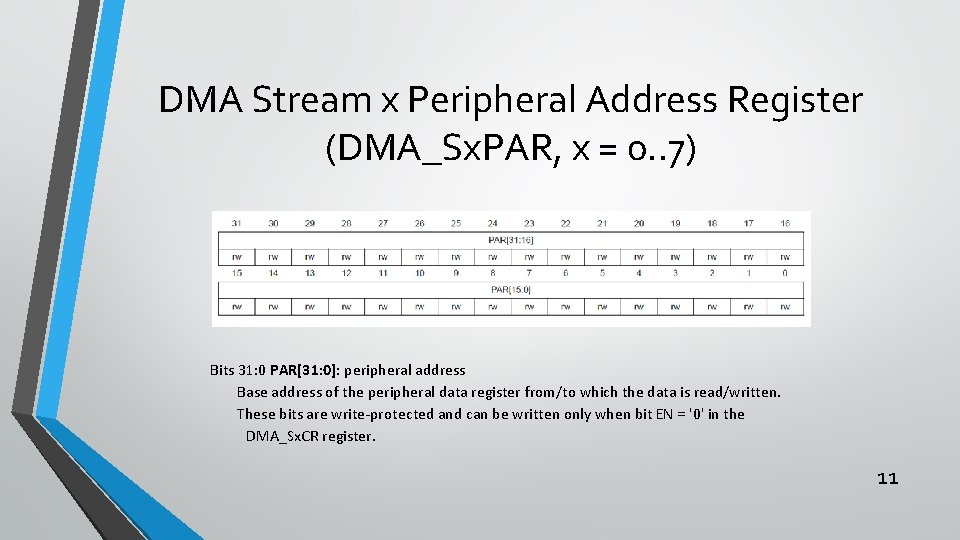
DMA Stream x Peripheral Address Register (DMA_Sx. PAR, x = 0. . 7) Bits 31: 0 PAR[31: 0]: peripheral address Base address of the peripheral data register from/to which the data is read/written. These bits are write-protected and can be written only when bit EN = '0' in the DMA_Sx. CR register. 11

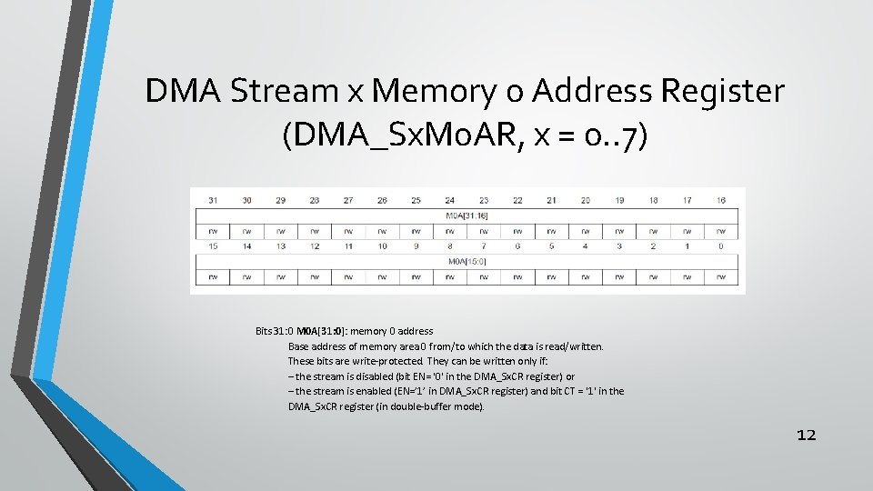
DMA Stream x Memory 0 Address Register (DMA_Sx. M 0 AR, x = 0. . 7) Bits 31: 0 M 0 A[31: 0]: memory 0 address Base address of memory area 0 from/to which the data is read/written. These bits are write-protected. They can be written only if: – the stream is disabled (bit EN= '0' in the DMA_Sx. CR register) or – the stream is enabled (EN=’ 1’ in DMA_Sx. CR register) and bit CT = '1' in the DMA_Sx. CR register (in double-buffer mode). 12

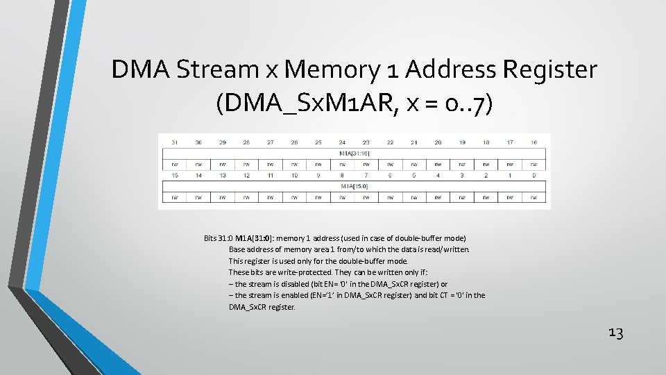
DMA Stream x Memory 1 Address Register (DMA_Sx. M 1 AR, x = 0. . 7) Bits 31: 0 M 1 A[31: 0]: memory 1 address (used in case of double-buffer mode) Base address of memory area 1 from/to which the data is read/written. This register is used only for the double-buffer mode. These bits are write-protected. They can be written only if: – the stream is disabled (bit EN= '0' in the DMA_Sx. CR register) or – the stream is enabled (EN=’ 1’ in DMA_Sx. CR register) and bit CT = '0' in the DMA_Sx. CR register. 13

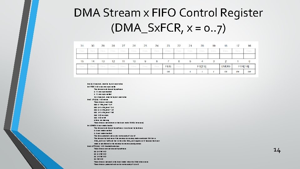
DMA Stream x FIFO Control Register (DMA_Sx. FCR, x = 0. . 7) Bits 31: 8 Reserved, must be kept at reset value. Bit 7 FEIE: FIFO error interrupt enable This bit is set and cleared by software. 0: FE interrupt disabled 1: FE interrupt enabled Bit 6 Reserved, must be kept at reset value. Bits 5: 3 FS[2: 0]: FIFO status These bits are read-only. 000: 0 < fifo_level < 1/4 001: 1/4 ≤ fifo_level < 1/2 010: 1/2 ≤ fifo_level < 3/4 011: 3/4 ≤ fifo_level < full 100: FIFO is empty 101: FIFO is full others: no meaning These bits are not relevant in the direct mode (DMDIS bit is zero). Bit 2 DMDIS: direct mode disable This bit is set and cleared by software. It can be set by hardware. 0: direct mode enabled 1: direct mode disabled This bit is protected and can be written only if EN is ‘ 0’. This bit is set by hardware if the memory-to-memory mode is selected (DIR bit in DMA_Sx. CR are “ 10”) and the EN bit in the DMA_Sx. CR register is ‘ 1’ because the direct mode is not allowed in the memory-to-memory configuration. Bits 1: 0 FTH[1: 0]: FIFO threshold selection These bits are set and cleared by software. 00: 1/4 full FIFO 01: 1/2 full FIFO 10: 3/4 full FIFO 11: full FIFO These bits are not used in the direct mode when the DMIS value is zero. These bits are protected and can be written only if EN is ‘ 0’. 14

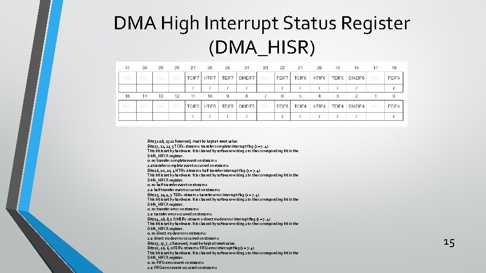
DMA High Interrupt Status Register (DMA_HISR) Bits 31: 28, 15: 12 Reserved, must be kept at reset value. Bits 27, 21, 11, 5 TCIFx: stream x transfer complete interrupt flag (x = 7. . 4) This bit is set by hardware. It is cleared by software writing 1 to the corresponding bit in the DMA_HIFCR register. 0: no transfer complete event on stream x 1: atransfer complete event occurred on stream x Bits 26, 20, 10, 4 HTIFx: stream x half transfer interrupt flag (x = 7. . 4) This bit is set by hardware. It is cleared by software writing 1 to the corresponding bit in the DMA_HIFCR register. 0: no half transfer event on stream x 1: a half transfer event occurred on stream x Bits 25, 19, 9, 3 TEIFx: stream x transfer error interrupt flag (x = 7. . 4) This bit is set by hardware. It is cleared by software writing 1 to the corresponding bit in the DMA_HIFCR register. 0: no transfer error on stream x 1: a transfer error occurred on stream x Bits 24, 18, 8, 2 DMEIFx: stream x direct mode error interrupt flag (x = 7. . 4) This bit is set by hardware. It is cleared by software writing 1 to the corresponding bit in the DMA_HIFCR register. 0: no direct mode error on stream x 1: a direct mode error occurred on stream x Bits 23, 17, 7, 1 Reserved, must be kept at reset value. Bits 22, 16, 6, 0 FEIFx: stream x FIFO error interrupt flag (x = 7. . 4) This bit is set by hardware. It is cleared by software writing 1 to the corresponding bit in the DMA_HIFCR register. 0: no FIFO error event on stream x 1: a FIFO error event occurred on stream x 15

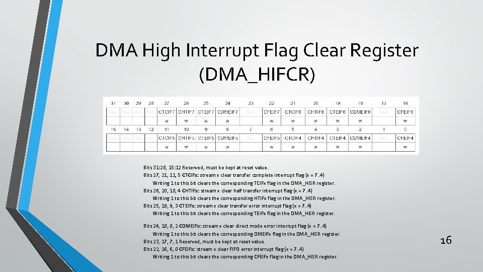
DMA High Interrupt Flag Clear Register (DMA_HIFCR) Bits 31: 28, 15: 12 Reserved, must be kept at reset value. Bits 27, 21, 11, 5 CTCIFx: stream x clear transfer complete interrupt flag (x = 7. . 4) Writing 1 to this bit clears the corresponding TCIFx flag in the DMA_HISR register. Bits 26, 20, 10, 4 CHTIFx: stream x clear half transfer interrupt flag (x = 7. . 4) Writing 1 to this bit clears the corresponding HTIFx flag in the DMA_HISR register. Bits 25, 19, 9, 3 CTEIFx: stream x clear transfer error interrupt flag (x = 7. . 4) Writing 1 to this bit clears the corresponding TEIFx flag in the DMA_HISR register. Bits 24, 18, 8, 2 CDMEIFx: stream x clear direct mode error interrupt flag (x = 7. . 4) Writing 1 to this bit clears the corresponding DMEIFx flag in the DMA_HISR register. Bits 23, 17, 7, 1 Reserved, must be kept at reset value. Bits 22, 16, 6, 0 CFEIFx: stream x clear FIFO error interrupt flag (x = 7. . 4) Writing 1 to this bit clears the corresponding CFEIFx flag in the DMA_HISR register. 16

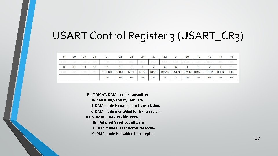
USART Control Register 3 (USART_CR 3) Bit 7 DMAT: DMA enable transmitter This bit is set/reset by software 1: DMA mode is enabled for transmission. 0: DMA mode is disabled for transmission. Bit 6 DMAR: DMA enable receiver This bit is set/reset by software 1: DMA mode is enabled for reception 0: DMA mode is disabled for reception 17