x HardwareLevel Performance Analysis of Platform IO PATRICK



- Slides: 23
x Hardware-Level Performance Analysis of Platform I/O PATRICK LU, ROMAN SUDARIKOV INTEL
Legal Disclaimer & Optimization Notice • Software and workloads used in performance tests may have been optimized for performance only on Intel microprocessors. Performance tests, such as SYSmark and Mobile. Mark, are measured using specific computer systems, components, software, operations and functions. Any change to any of those factors may cause the results to vary. You should consult other information and performance tests to assist you in fully evaluating your contemplated purchases, including the performance of that product when combined with other products. For more complete information visit www. intel. com/benchmarks. • INFORMATION IN THIS DOCUMENT IS PROVIDED “AS IS”. NO LICENSE, EXPRESS OR IMPLIED, BY ESTOPPEL OR OTHERWISE, TO ANY INTELLECTUAL PROPERTY RIGHTS IS GRANTED BY THIS DOCUMENT. INTEL ASSUMES NO LIABILITY WHATSOEVER AND INTEL DISCLAIMS ANY EXPRESS OR IMPLIED WARRANTY, RELATING TO THIS INFORMATION INCLUDING LIABILITY OR WARRANTIES RELATING TO FITNESS FOR A PARTICULAR PURPOSE, MERCHANTABILITY, OR INFRINGEMENT OF ANY PATENT, COPYRIGHT OR OTHER INTELLECTUAL PROPERTY RIGHT. • Copyright © 2018, Intel Corporation. All rights reserved. Intel, Pentium, Xeon Phi, Core, VTune, Cilk, and the Intel logo are trademarks of Intel Corporation in the U. S. and other countries. Optimization Notice Intel’s compilers may or may not optimize to the same degree for non-Intel microprocessors for optimizations that are not unique to Intel microprocessors. These optimizations include SSE 2, SSE 3, and SSSE 3 instruction sets and other optimizations. Intel does not guarantee the availability, functionality, or effectiveness of any optimization on microprocessors not manufactured by Intel. Microprocessor-dependent optimizations in this product are intended for use with Intel microprocessors. Certain optimizations not specific to Intel microarchitecture are reserved for Intel microprocessors. Please refer to the applicable product User and Reference Guides for more information regarding the specific instruction sets covered by this notice. Notice revision #20110804 2
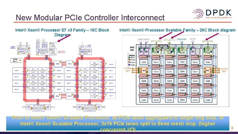
New Modular PCIe Controller Interconnect Intel® Xeon® Processor E 7 v 3 Family – 18 C Block Diagram Intel® Xeon® Processor Scalable Family – 28 C Block diagram Prior to Intel® Xeon® Scalable Processor, all PCIe lanes aggregated to single ring stop. In Intel® Xeon® Scalable Processor, 3 x 16 PCIe lanes split to three mesh stop. (higher concurrent I/O) 3
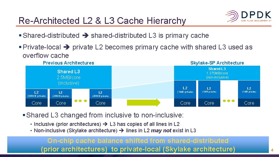
Re-Architected L 2 & L 3 Cache Hierarchy § Shared-distributed shared-distributed L 3 is primary cache § Private-local private L 2 becomes primary cache with shared L 3 used as overflow cache Previous Architectures Skylake-SP Architecture Shared L 3 1. 375 MB/core (non-inclusive) Shared L 3 2. 5 MB/core (inclusive) L 2 L 2 (256 KB private) (256 KB private ) Core L 2 L 2 (1 MB private) Core § Shared L 3 changed from inclusive to non-inclusive: • Inclusive (prior architectures) L 3 has copies of all lines in L 2 • Non-inclusive (Skylake architecture) lines in L 2 may not exist in L 3 On-chip cache balance shifted from shared-distributed (prior architectures) to private-local (Skylake architecture) 4
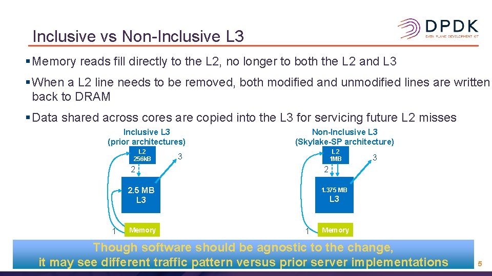
Inclusive vs Non-Inclusive L 3 § Memory reads fill directly to the L 2, no longer to both the L 2 and L 3 § When a L 2 line needs to be removed, both modified and unmodified lines are written back to DRAM § Data shared across cores are copied into the L 3 for servicing future L 2 misses Inclusive L 3 (prior architectures) L 2 256 k. B Non-Inclusive L 3 (Skylake-SP architecture) L 2 1 MB 3 2 2 2. 5 MB L 3 1 Memory 3 1. 375 MB L 3 1 Memory Though software should be agnostic to the change, it may see different traffic pattern versus prior server implementations 5
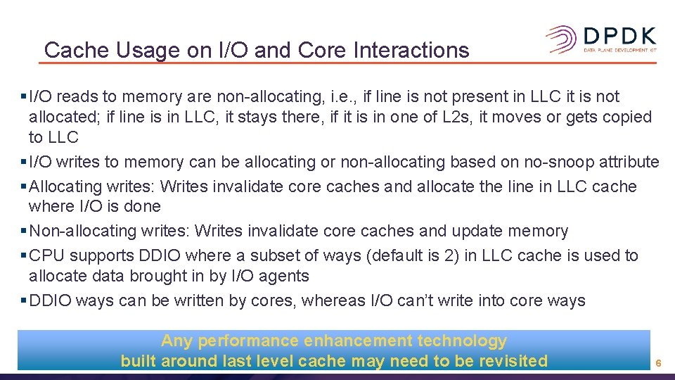
Cache Usage on I/O and Core Interactions § I/O reads to memory are non-allocating, i. e. , if line is not present in LLC it is not allocated; if line is in LLC, it stays there, if it is in one of L 2 s, it moves or gets copied to LLC § I/O writes to memory can be allocating or non-allocating based on no-snoop attribute § Allocating writes: Writes invalidate core caches and allocate the line in LLC cache where I/O is done § Non-allocating writes: Writes invalidate core caches and update memory § CPU supports DDIO where a subset of ways (default is 2) in LLC cache is used to allocate data brought in by I/O agents § DDIO ways can be written by cores, whereas I/O can’t write into core ways Any performance enhancement technology built around last level cache may need to be revisited 6
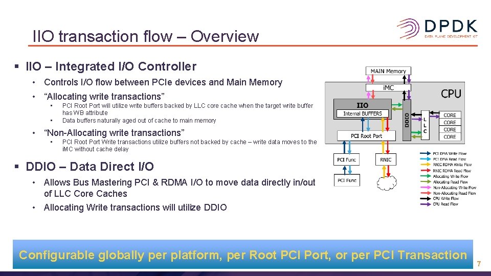
IIO transaction flow – Overview § IIO – Integrated I/O Controller • Controls I/O flow between PCIe devices and Main Memory • “Allocating write transactions” • • PCI Root Port will utilize write buffers backed by LLC core cache when the target write buffer has WB attribute Data buffers naturally aged out of cache to main memory • “Non-Allocating write transactions” • PCI Root Port Write transactions utilize buffers not backed by cache – write data moves to the i. MC without cache delay § DDIO – Data Direct I/O • Allows Bus Mastering PCI & RDMA I/O to move data directly in/out of LLC Core Caches • Allocating Write transactions will utilize DDIO Configurable globally per platform, per Root PCI Port, or per PCI Transaction 7
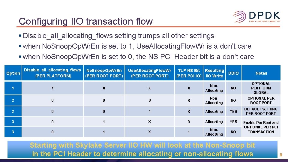
Configuring IIO transaction flow § Disable_allocating_flows setting trumps all other settings § when No. Snoop. Op. Wr. En is set to 1, Use. Allocating. Flow. Wr is a don’t care § when No. Snoop. Op. Wr. En is set to 0, the NS PCI Header bit is a don’t care Option Disable_allocating_flows (PER PLATFORM) No. Snoop. Op. Wr. En (PER ROOT PORT) Use. Allocating. Flow. Wr (PER ROOT PORT) TLP NS Bit Resulting (PER PCI IO) IIO Write DDIO Notes NO OPTIONAL PLATFORM GLOBAL 1 1 X X X Non. Allocating 2 0 0 0 X Non. Allocating NO OPTIONAL PER ROOT PORT 2 0 0 1 X Allocating YES DEFAULT SETTING PER ROOT PORT 3 0 1 X 0 Allocating YES 3 0 1 X 1 Non. Allocating NO Enable Per Root and OPTIONAL PER PCI TRANSACTION Starting with Skylake Server IIO HW will look at the Non-Snoop bit in the PCI Header to determine allocating or non-allocating flows 8
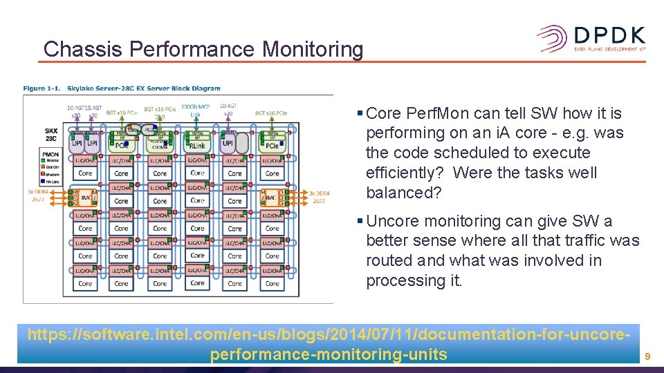
Chassis Performance Monitoring § Core Perf. Mon can tell SW how it is performing on an i. A core - e. g. was the code scheduled to execute efficiently? Were the tasks well balanced? § Uncore monitoring can give SW a better sense where all that traffic was routed and what was involved in processing it. https: //software. intel. com/en-us/blogs/2014/07/11/documentation-for-uncoreperformance-monitoring-units 9
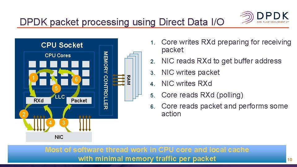
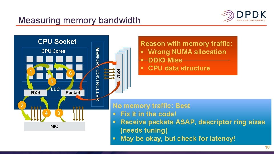
DPDK packet processing using Direct Data I/O CPU Socket 6 5 LLC RXd 2 4 1 Packet RAM 1 MEMORY CONTROLLER CPU Cores 1. Core writes RXd preparing for receiving packet 2. NIC reads RXd to get buffer address 3. NIC writes packet 4. NIC writes RXd 5. Core reads RXd (polling) 6. Core reads packet and performs some action 3 NIC Most of software thread work in CPU core and local cache with minimal memory traffic per packet 10
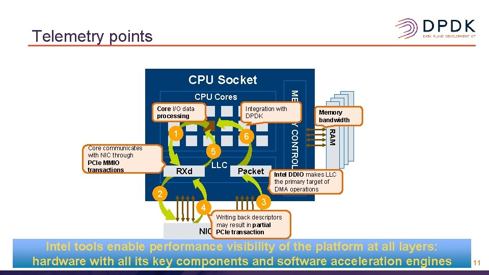
Telemetry points CPU Socket Integration with DPDK Core I/O data processing Core communicates with NIC through PCIe MMIO transactions 6 5 LLC RXd 2 4 1 NIC Packet Memory bandwidth RAM 1 MEMORY CONTROLLER CPU Cores Intel DDIO makes LLC the primary target of DMA operations 3 Writing back descriptors may result in partial PCIe transaction Intel tools enable performance visibility of the platform at all layers: hardware with all its key components and software acceleration engines 11
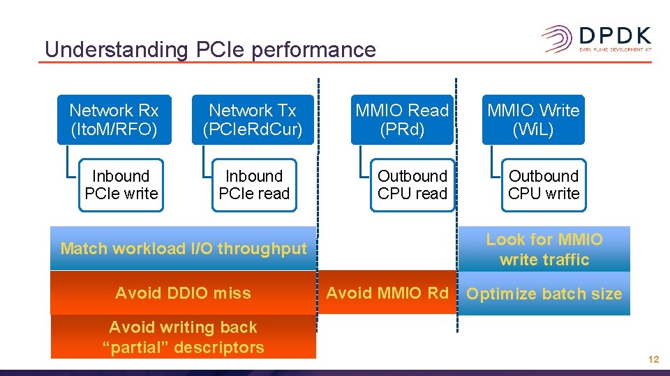
Understanding PCIe performance Network Rx (Ito. M/RFO) Inbound PCIe write Network Tx (PCIe. Rd. Cur) Inbound PCIe read MMIO Read (PRd) MMIO Write (Wi. L) Outbound CPU read Outbound CPU write Look for MMIO write traffic Match workload I/O throughput Avoid DDIO miss Avoid writing back “partial” descriptors Avoid MMIO Rd Optimize batch size 12
Measuring memory bandwidth CPU Socket 6 5 LLC RXd 2 4 1 3 NIC Packet RAM 1 MEMORY CONTROLLER CPU Cores Reason with memory traffic: § Wrong NUMA allocation § DDIO Miss § CPU data structure No memory traffic: Best § Fix it in the code! § Receive packets ASAP, descriptor ring sizes (needs tuning) § May be okay, but check for latency! 13
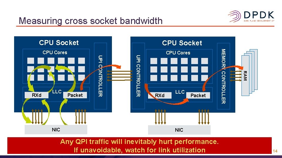
Measuring cross socket bandwidth CPU Socket 1 RXd LLC Packet RAM NIC Packet CPU Cores MEMORY CONTROLLER 1 LLC UPI CONTROLLER RXd UPI CONTROLLER CPU Cores NIC Any QPI traffic will inevitably hurt performance. If unavoidable, watch for link utilization 14
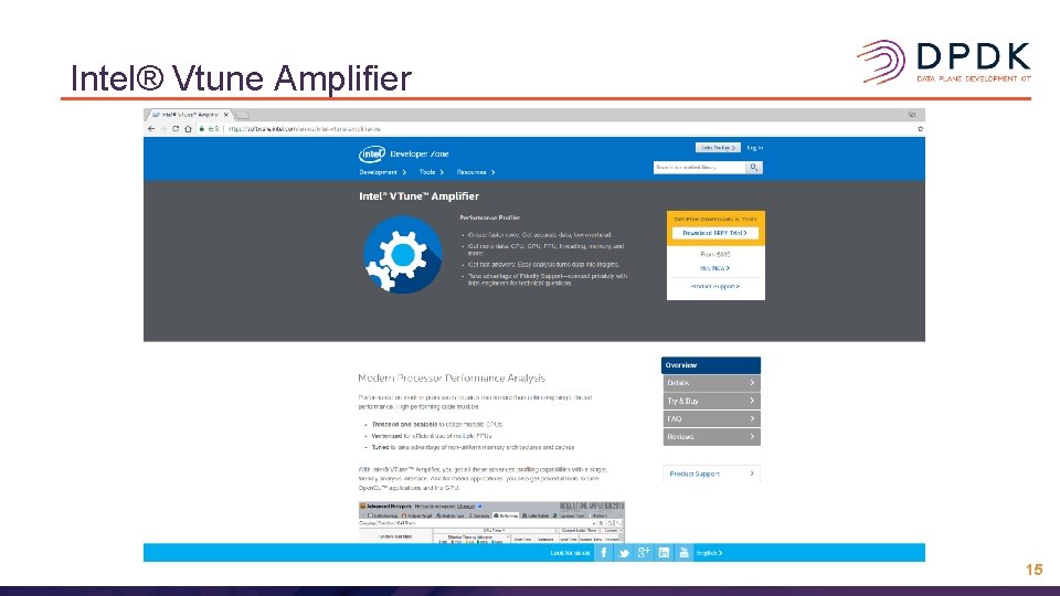
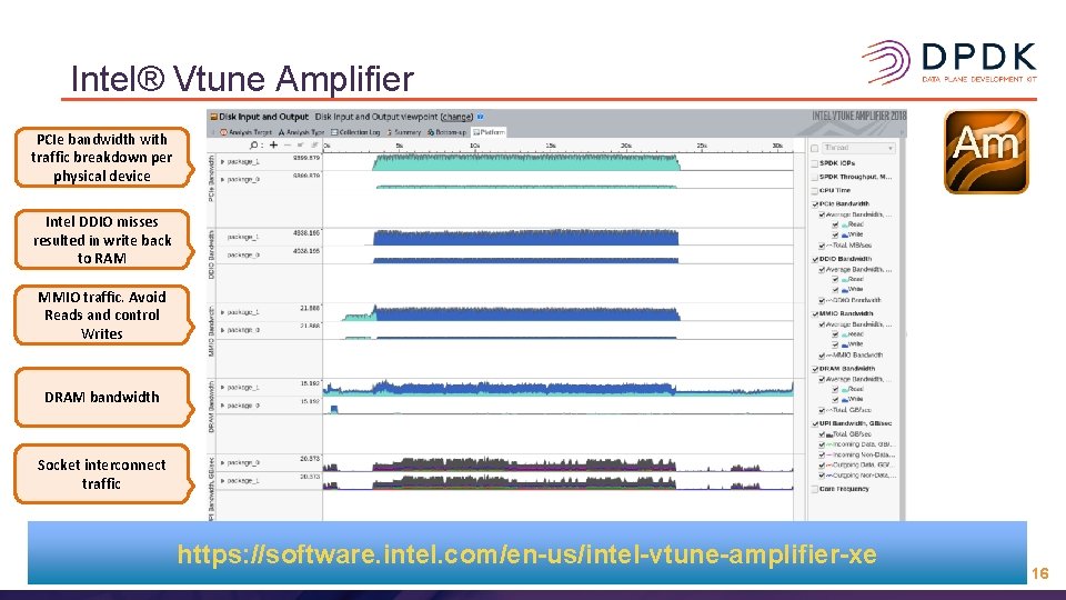
Intel® Vtune Amplifier 15
Intel® Vtune Amplifier PCIe bandwidth with traffic breakdown per physical device Intel DDIO misses resulted in write back to RAM MMIO traffic. Avoid Reads and control Writes DRAM bandwidth Socket interconnect traffic 1 https: //software. intel. com/en-us/intel-vtune-amplifier-xe 16
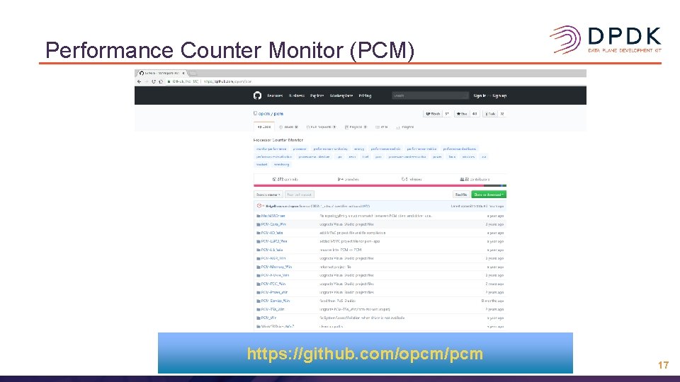
Performance Counter Monitor (PCM) https: //github. com/opcm/pcm 17
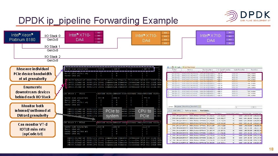
DPDK ip_pipeline Forwarding Example Intel® Xeon® Platinum 8180 IIO Stack 0 Gen 3 x 8 Intel® X 710 DA 4 10 G 10 G Intel® X 710 DA 4 10 G 10 G IIO Stack 1 Gen 3 x 8 IIO Stack 2 Gen 3 x 8 Measure individual PCIe device bandwidth at x 4 granularity Enumerate downstream devices behind each IIO Stack Monitor both inbound/outbound at DWord granularity PCIe to system CPU to PCIe Can monitor VT-d IOTLB miss rate (op. Code. txt) 18
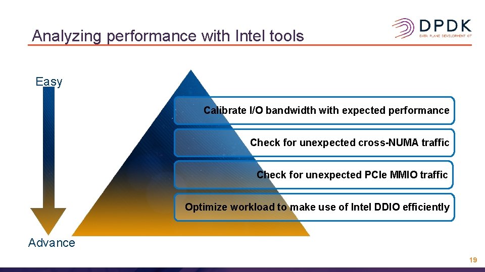
Analyzing performance with Intel tools Easy Calibrate I/O bandwidth with expected performance Check for unexpected cross-NUMA traffic Check for unexpected PCIe MMIO traffic Optimize workload to make use of Intel DDIO efficiently 1 Advance 19
Patrick Lu PATRICK. LU@INTEL. COM Questions? Roman Sudarikov ROMAN. SUDARIKOV@INTEL. COM
Backup
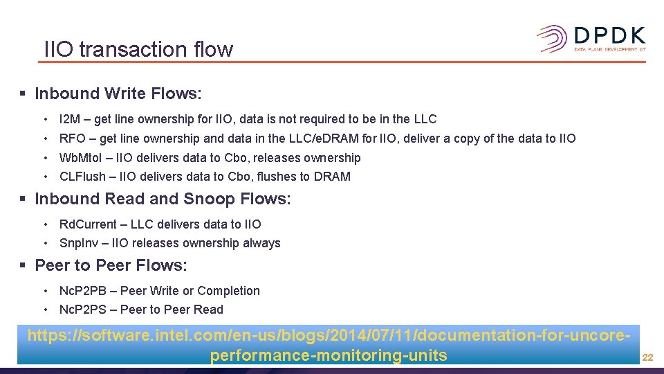
IIO transaction flow § Inbound Write Flows: • • I 2 M – get line ownership for IIO, data is not required to be in the LLC RFO – get line ownership and data in the LLC/e. DRAM for IIO, deliver a copy of the data to IIO Wb. Mto. I – IIO delivers data to Cbo, releases ownership CLFlush – IIO delivers data to Cbo, flushes to DRAM § Inbound Read and Snoop Flows: • Rd. Current – LLC delivers data to IIO • Snp. Inv – IIO releases ownership always § Peer to Peer Flows: • Nc. P 2 PB – Peer Write or Completion • Nc. P 2 PS – Peer to Peer Read https: //software. intel. com/en-us/blogs/2014/07/11/documentation-for-uncoreperformance-monitoring-units 22
Configuring IIO transaction flow § Option 1: global per platform § Option 2: per root port § Option 3: per pci transaction 23