Working Towards Large Area PicosecondLevel Photodetectors Matthew Wetstein
- Slides: 30

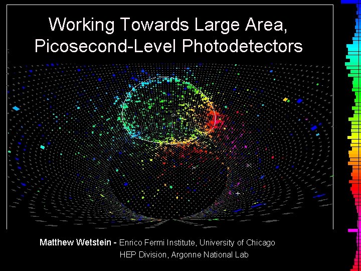
Working Towards Large Area, Picosecond-Level Photodetectors Matthew Wetstein - Enrico Fermi Institute, University of Chicago HEP Division, Argonne National Lab

LAPPD Collaboration: Large Area Picosecond Photodetectors The LAPPD Collaboration Large Area Picsecond Photodetector Collaboration John Anderson, Karen Byrum, Gary Drake, Henry Frisch, Edward May, Alexander Paramonov, Mayly Sanchez, Robert Stanek, Robert G. Wagner, Hendrik Weerts, Matthew Wetstein, Zikri Zusof High Energy Physics Division, Argonne National Laboratory, Argonne, IL Bernhard Adams, Klaus Attenkofer, Mattieu Chollet Advanced Photon Source Division, Argonne National Laboratory, Argonne, IL Zeke Insepov Mathematics and Computer Sciences Division, Argonne National Laboratory, Argonne, IL Mane Anil, Jeffrey Elam, Joseph Libera, Qing Peng Energy Systems Division, Argonne National Laboratory, Argonne, IL Michael Pellin, Thomas Prolier, Igor Veryovkin, Hau Wang, Alexander Zinovev Materials Science Division, Argonne National Laboratory, Argonne, IL Dean Walters Nuclear Engineering Division, Argonne National Laboratory, Argonne, IL David Beaulieu, Neal Sullivan, Ken Stenton • Newly funded (end of August) by DOE and NSF • 4 National Labs • 5 Divisions at Argonne • 3 US small companies; • Electronics expertise at Universities of Chicago and Hawaii Arradiance Inc. , Sudbury, MA Sam Asare, Michael Baumer, Mircea Bogdan, Henry Frisch, Jean-Francois Genat, Herve Grabas, Mary Heintz, Sam Meehan, Richard Northrop, Eric Oberla, Fukun Tang, Matthew Wetstein, Dai Zhongtian Enrico Fermi Institute, University of Chicago, IL Erik Ramberg, Anatoly Ronzhin, Greg Sellberg Fermi National Accelerator Laboratory, Batavia, IL James Kennedy, Kurtis Nishimura, Marc Rosen, Larry Ruckman, Gary Varner University of Hawaii, Honolulu, HI Robert Abrams, valentin Ivanov, Thomas Roberts Muons, Inc. , Batavia, IL Jerry Va’vra SLAC National Accelerator Laboratory, Menlo Park, CA Oswald Siegmund, Anton Tremsin Space Sciences Laboratory, University of California, Berkeley, CA Dimitri Routkevitch Synkera Technologies Inc. , Longmont, CO Goals: • Exploit advances in material science and nanotechnology to develop new, batch methods for producing cheap, large area MCPs. • To develop a commercializable product on a three year time scale. David Forbush, Tianchi Zhao Department of Physics, University of Washington, Seattle, WA NNN 09 2

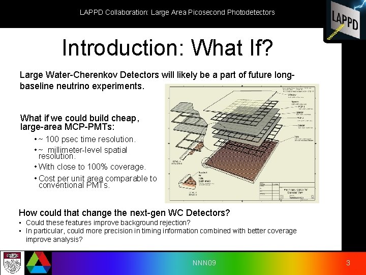
LAPPD Collaboration: Large Area Picosecond Photodetectors Introduction: What If? Large Water-Cherenkov Detectors will likely be a part of future longbaseline neutrino experiments. What if we could build cheap, large-area MCP-PMTs: • ~ 100 psec time resolution. • ~ millimeter-level spatial resolution. • With close to 100% coverage. • Cost per unit area comparable to conventional PMTs. How could that change the next-gen WC Detectors? • Could these features improve background rejection? • In particular, could more precision in timing information combined with better coverage improve analysis? NNN 09 3

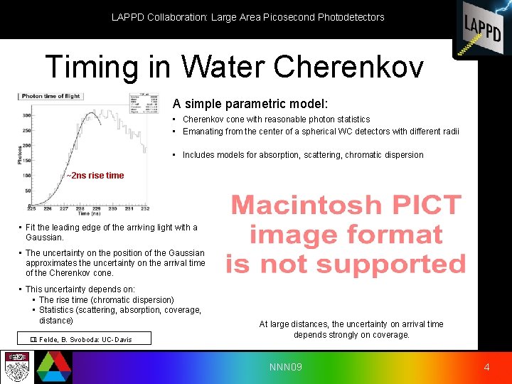
LAPPD Collaboration: Large Area Picosecond Photodetectors Timing in Water Cherenkov A simple parametric model: • Cherenkov cone with reasonable photon statistics • Emanating from the center of a spherical WC detectors with different radii • Includes models for absorption, scattering, chromatic dispersion ~2 ns rise time • Fit the leading edge of the arriving light with a Gaussian. • The uncertainty on the position of the Gaussian approximates the uncertainty on the arrival time of the Cherenkov cone. • This uncertainty depends on: • The rise time (chromatic dispersion) • Statistics (scattering, absorption, coverage, distance) � J. Felde, B. Svoboda: UC-Davis At large distances, the uncertainty on arrival time depends strongly on coverage. NNN 09 4

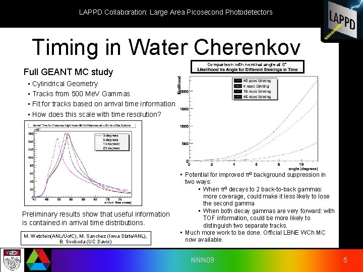
LAPPD Collaboration: Large Area Picosecond Photodetectors Timing in Water Cherenkov Comparison with nominal angle at 0° Full GEANT MC study • Cylindrical Geometry • Tracks from 500 Me. V Gammas • Fit for tracks based on arrival time information • How does this scale with time resolution? Preliminary results show that useful information is contained in arrival time distributions. M. Wetstein(ANL/Uof. C), M. Sanchez (Iowa State/ANL), B. Svoboda (UC Davis) • Potential for improved π0 background suppression in two ways: • When π0 decays to 2 back-to-back gammas: more coverage, could make it less likely to lose the second gamma • When both decay gammas are very forward: with TOF information, could be more likely to distinguish two separate tracks. • Much more work to be done. Official LBNE WCh MC now available. NNN 09 5

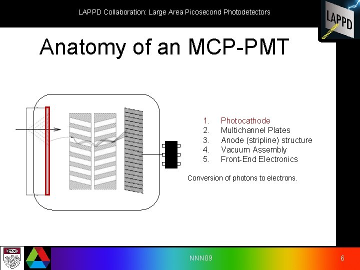
LAPPD Collaboration: Large Area Picosecond Photodetectors Anatomy of an MCP-PMT 1. 2. 3. 4. 5. Photocathode Multichannel Plates Anode (stripline) structure Vacuum Assembly Front-End Electronics Conversion of photons to electrons. NNN 09 6

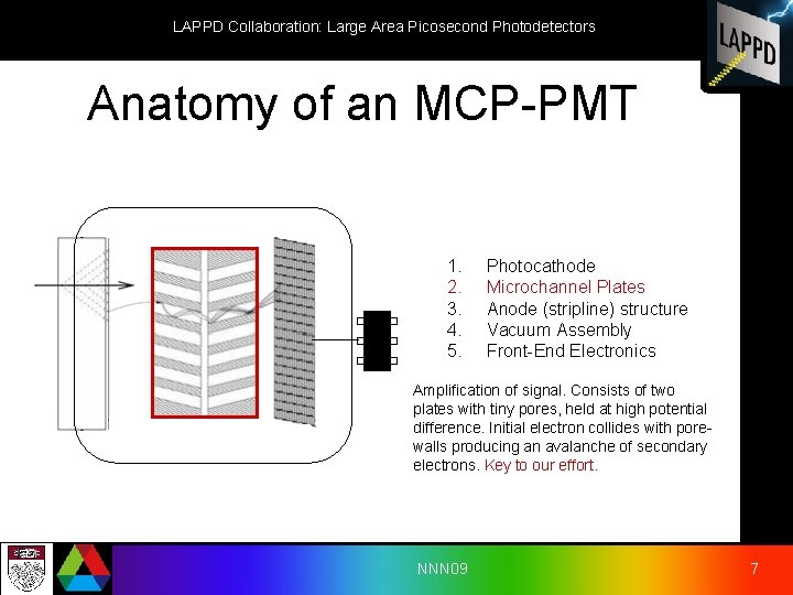
LAPPD Collaboration: Large Area Picosecond Photodetectors Anatomy of an MCP-PMT 1. 2. 3. 4. 5. Photocathode Microchannel Plates Anode (stripline) structure Vacuum Assembly Front-End Electronics Amplification of signal. Consists of two plates with tiny pores, held at high potential difference. Initial electron collides with porewalls producing an avalanche of secondary electrons. Key to our effort. NNN 09 7

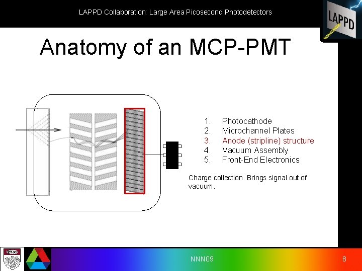
LAPPD Collaboration: Large Area Picosecond Photodetectors Anatomy of an MCP-PMT 1. 2. 3. 4. 5. Photocathode Microchannel Plates Anode (stripline) structure Vacuum Assembly Front-End Electronics Charge collection. Brings signal out of vacuum. NNN 09 8

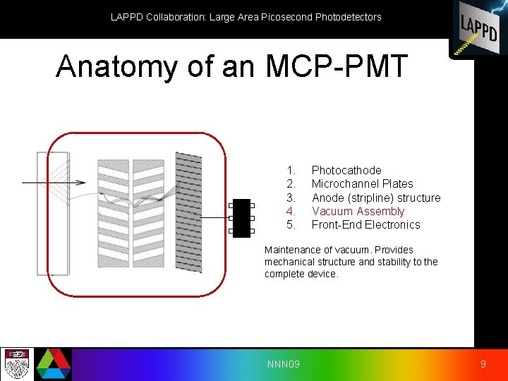
LAPPD Collaboration: Large Area Picosecond Photodetectors Anatomy of an MCP-PMT 1. 2. 3. 4. 5. Photocathode Microchannel Plates Anode (stripline) structure Vacuum Assembly Front-End Electronics Maintenance of vacuum. Provides mechanical structure and stability to the complete device. NNN 09 9

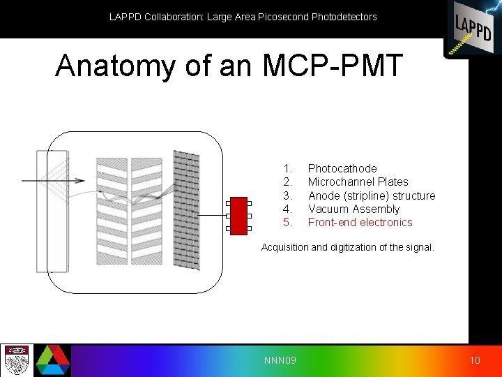
LAPPD Collaboration: Large Area Picosecond Photodetectors Anatomy of an MCP-PMT 1. 2. 3. 4. 5. Photocathode Microchannel Plates Anode (stripline) structure Vacuum Assembly Front-end electronics Acquisition and digitization of the signal. NNN 09 10

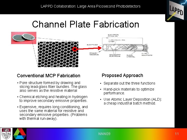
LAPPD Collaboration: Large Area Picosecond Photodetectors Channel Plate Fabrication Conventional MCP Fabrication • Pore structure formed by drawing and slicing lead-glass fiber bundles. The glass also serves as the resistive material • Chemical etching and heating in hydrogen to improve secondary emissive properties. • Expensive, requires long conditioning, and uses the same material for resistive and secondary emissive properties. (Problems with thermal run-away). Proposed Approach • Separate out the three functions • Hand-pick materials to optimize performance. • Use Atomic Layer Deposition (ALD): a cheap industrial batch method. NNN 09 11

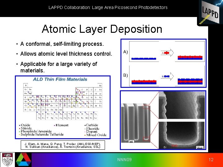
LAPPD Collaboration: Large Area Picosecond Photodetectors Atomic Layer Deposition • A conformal, self-limiting process. • Allows atomic level thickness control. • Applicable for a large variety of materials. J. Elam, A. Mane, Q. Peng, T. Prolier (ANL: ESD/HEP), N. Sullivan (Arradiance), A. Tremsin (Arradiance, SSL) NNN 09 12

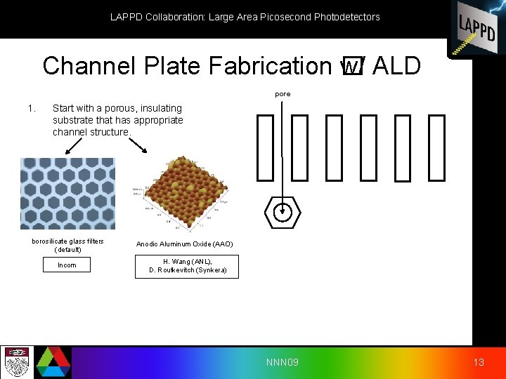
LAPPD Collaboration: Large Area Picosecond Photodetectors Channel Plate Fabrication � w/ ALD pore 1. Start with a porous, insulating substrate that has appropriate channel structure. borosilicate glass filters (default) Incom Anodic Aluminum Oxide (AAO) H. Wang (ANL), D. Routkevitch (Synkera) NNN 09 13

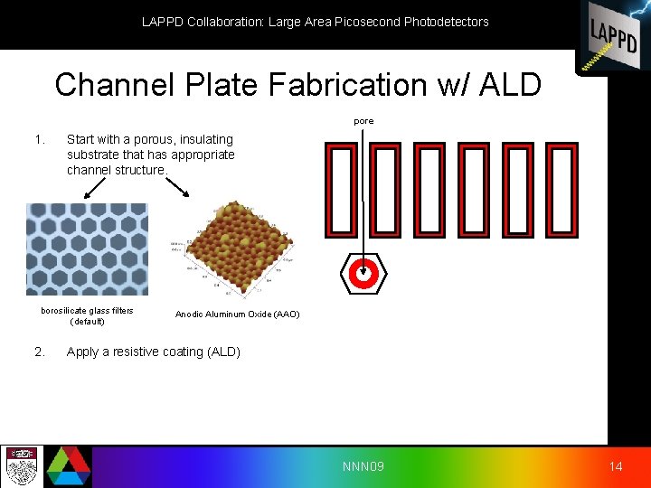
LAPPD Collaboration: Large Area Picosecond Photodetectors Channel Plate Fabrication w/ ALD pore 1. Start with a porous, insulating substrate that has appropriate channel structure. borosilicate glass filters (default) 2. Anodic Aluminum Oxide (AAO) Apply a resistive coating (ALD) NNN 09 14

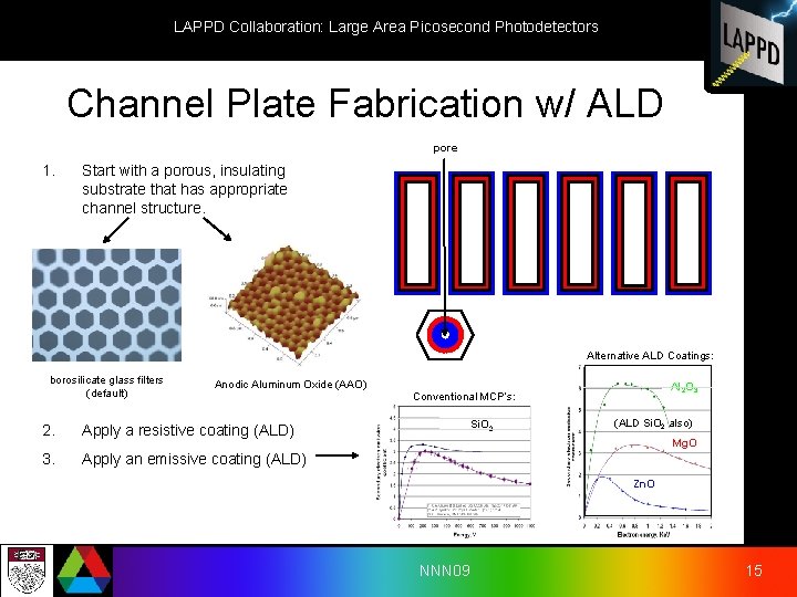
LAPPD Collaboration: Large Area Picosecond Photodetectors Channel Plate Fabrication w/ ALD pore 1. Start with a porous, insulating substrate that has appropriate channel structure. Alternative ALD Coatings: borosilicate glass filters (default) Anodic Aluminum Oxide (AAO) 2. Apply a resistive coating (ALD) 3. Apply an emissive coating (ALD) Al 2 O 3 Conventional MCP’s: Si. O 2 (ALD Si. O 2 also) Mg. O Zn. O NNN 09 15

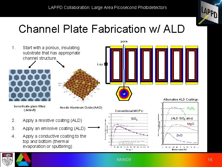
LAPPD Collaboration: Large Area Picosecond Photodetectors Channel Plate Fabrication w/ ALD pore 1. Start with a porous, insulating substrate that has appropriate channel structure. 1 KV Alternative ALD Coatings: borosilicate glass filters (default) Anodic Aluminum Oxide (AAO) 2. Apply a resistive coating (ALD) 3. Apply an emissive coating (ALD) 4. Apply a conductive coating to the top and bottom (thermal evaporation or sputtering) Al 2 O 3 Conventional MCP’s: Si. O 2 (ALD Si. O 2 also) Mg. O Zn. O NNN 09 16

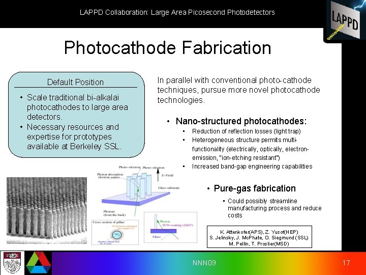
LAPPD Collaboration: Large Area Picosecond Photodetectors Photocathode Fabrication Default Position • Scale traditional bi-alkalai photocathodes to large area detectors. • Necessary resources and expertise for prototypes available at Berkeley SSL. In parallel with conventional photo-cathode techniques, pursue more novel photocathode technologies. • Nano-structured photocathodes: • • • Reduction of reflection losses (light trap) Heterogeneous structure permits multifunctionality (electrically, optically, electronemission, “ion-etching resistant”) Increased band-gap engineering capabilities • Pure-gas fabrication • Could possibly streamline manufacturing process and reduce costs K. Attenkofer(APS), Z. Yusof(HEP) S. Jelinsky, J. Mc. Phate, O. Siegmund (SSL) M. Pellin, T. Proslier(MSD) NNN 09 17

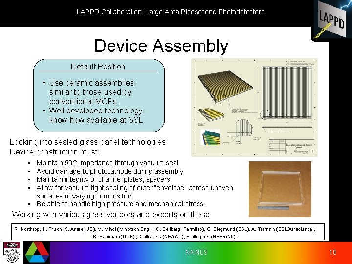
LAPPD Collaboration: Large Area Picosecond Photodetectors Device Assembly Default Position • Use ceramic assemblies, similar to those used by conventional MCPs. • Well developed technology, know-how available at SSL Looking into sealed glass-panel technologies. Device construction must: • • Maintain 50Ω impedance through vacuum seal Avoid damage to photocathode during assembly Maintain integrity of channel plates, spacers Allow for vacuum tight sealing of outer “envelope” across uneven surfaces of varying composition • Be able to handle high pressure and mechanical stress. Working with various glass vendors and experts on these. R. Northrop, H. Frisch, S. Asare (UC), M. Minot (Minotech Eng. ), G. Sellberg (Fermilab), O. Siegmund (SSL), A. Tremsin (SSL/Arradiance), R. Barwhani (UCB) , D. Walters (NE/ANL), R. Wagner (HEP/ANL), NNN 09 18

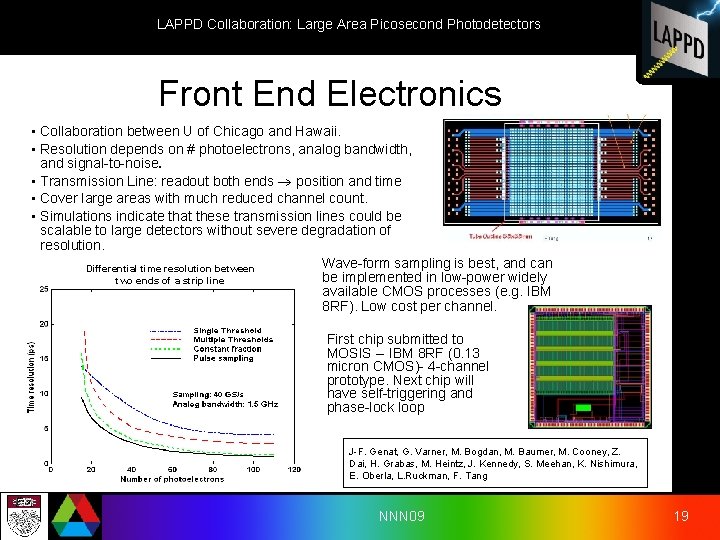
LAPPD Collaboration: Large Area Picosecond Photodetectors Front End Electronics • Collaboration between U of Chicago and Hawaii. • Resolution depends on # photoelectrons, analog bandwidth, and signal-to-noise. • Transmission Line: readout both ends position and time • Cover large areas with much reduced channel count. • Simulations indicate that these transmission lines could be scalable to large detectors without severe degradation of resolution. Wave-form sampling is best, and can Differential time resolution between be implemented in low-power widely two ends of a strip line available CMOS processes (e. g. IBM 8 RF). Low cost per channel. First chip submitted to MOSIS -- IBM 8 RF (0. 13 micron CMOS)- 4 -channel prototype. Next chip will have self-triggering and phase-lock loop J-F. Genat, G. Varner, M. Bogdan, M. Baumer, M. Cooney, Z. Dai, H. Grabas, M. Heintz, J. Kennedy, S. Meehan, K. Nishimura, E. Oberla, L. Ruckman, F. Tang NNN 09 19

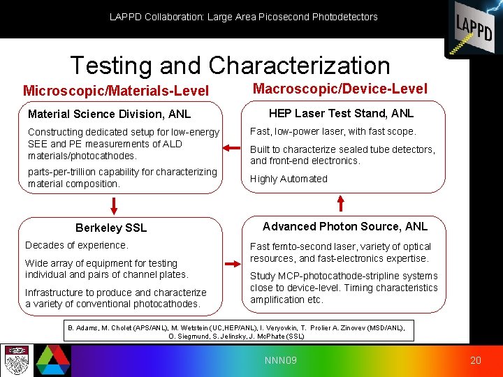
LAPPD Collaboration: Large Area Picosecond Photodetectors Testing and Characterization Microscopic/Materials-Level Material Science Division, ANL Constructing dedicated setup for low-energy SEE and PE measurements of ALD materials/photocathodes. parts-per-trillion capability for characterizing material composition. Berkeley SSL Decades of experience. Wide array of equipment for testing individual and pairs of channel plates. Infrastructure to produce and characterize a variety of conventional photocathodes. Macroscopic/Device-Level HEP Laser Test Stand, ANL Fast, low-power laser, with fast scope. Built to characterize sealed tube detectors, and front-end electronics. Highly Automated Advanced Photon Source, ANL Fast femto-second laser, variety of optical resources, and fast-electronics expertise. Study MCP-photocathode-stripline systems close to device-level. Timing characteristics amplification etc. B. Adams, M. Cholet (APS/ANL), M. Wetstein (UC, HEP/ANL), I. Veryovkin, T. Prolier A. Zinovev (MSD/ANL), O. Siegmund, S. Jelinsky, J. Mc. Phate (SSL) NNN 09 20

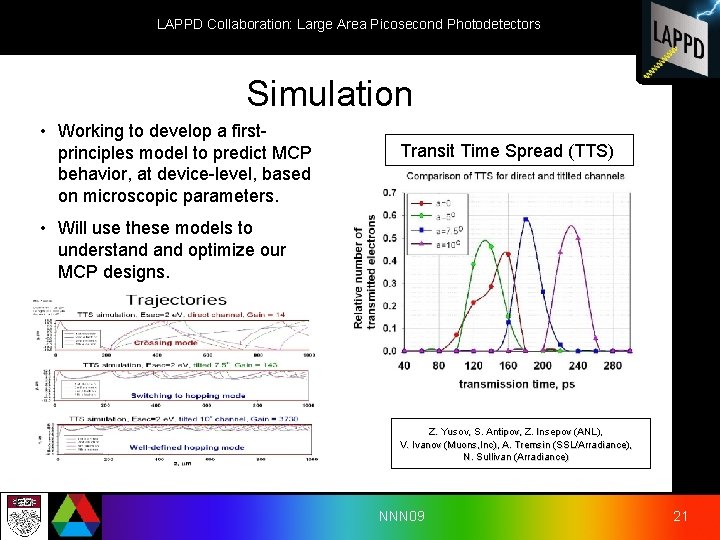
LAPPD Collaboration: Large Area Picosecond Photodetectors Simulation • Working to develop a firstprinciples model to predict MCP behavior, at device-level, based on microscopic parameters. Transit Time Spread (TTS) • Will use these models to understand optimize our MCP designs. Z. Yusov, S. Antipov, Z. Insepov (ANL), V. Ivanov (Muons, Inc), A. Tremsin (SSL/Arradiance), N. Sullivan (Arradiance)) NNN 09 21

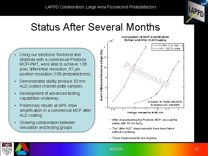
LAPPD Collaboration: Large Area Picosecond Photodetectors Status After Several Months • Using our electronic front-end and striplines with a commercial Photonis MCP-PMT, were able to achieve 1. 95 psec differential resolution, 97 µm position resolution (158 photoelectrons). Pre • Demonstrated ability produce 33 mm ALD coated channel-plate samples. • Development of advanced testing capabilities underway. ina ry B. Adams, M. Chollet (ANL/APS), M. Wetstein (UC, ANL/HEP) • Preliminary results at APS show amplification in a commercial MCP after ALD coating. • Growing collaboration between simulation and testing groups. lim • After characterizing the Photonis MCP, we coat the plates with 10 nm Al 2 O 3. • The “after-ALD” measurements have been taken without scrubbing. • These measurements are ongoing. NNN 09 22

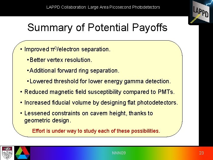
LAPPD Collaboration: Large Area Picosecond Photodetectors Summary of Potential Payoffs • Improved π0/electron separation. • Better vertex resolution. • Additional forward ring separation. • Lowered threshold for lower energy gamma detection. • Reduced magnetic field susceptibility compared to PMTs. • Increased fiducial volume by designing flat photodetectors. • Lessened constraints on cavern height, thanks to geometric design. Effort is under way to study each of these possibilities. NNN 09 23

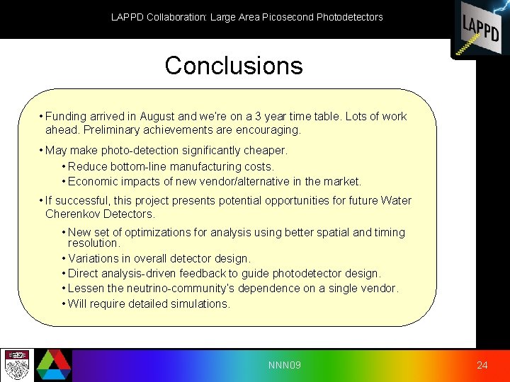
LAPPD Collaboration: Large Area Picosecond Photodetectors Conclusions • Funding arrived in August and we’re on a 3 year time table. Lots of work ahead. Preliminary achievements are encouraging. • May make photo-detection significantly cheaper. • Reduce bottom-line manufacturing costs. • Economic impacts of new vendor/alternative in the market. • If successful, this project presents potential opportunities for future Water Cherenkov Detectors. • New set of optimizations for analysis using better spatial and timing resolution. • Variations in overall detector design. • Direct analysis-driven feedback to guide photodetector design. • Lessen the neutrino-community’s dependence on a single vendor. • Will require detailed simulations. NNN 09 24

LAPPD Collaboration: Large Area Picosecond Photodetectors Thanks • NNN 09 for hosting. • LAPPD collaboration for their help and hard work. • Mayly Sanchez, Henry Frisch, Bob Svoboda for their feedback and guidance. NNN 09 25

LAPPD Collaboration: Large Area Picosecond Photodetectors Backup Slides NNN 09 26

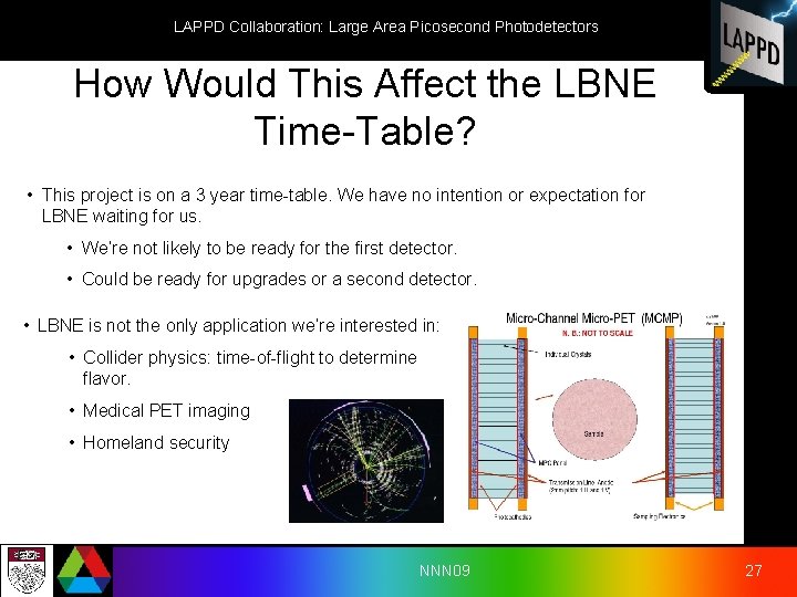
LAPPD Collaboration: Large Area Picosecond Photodetectors How Would This Affect the LBNE Time-Table? • This project is on a 3 year time-table. We have no intention or expectation for LBNE waiting for us. • We’re not likely to be ready for the first detector. • Could be ready for upgrades or a second detector. • LBNE is not the only application we’re interested in: • Collider physics: time-of-flight to determine flavor. • Medical PET imaging • Homeland security NNN 09 27

LAPPD Collaboration: Large Area Picosecond Photodetectors How Much Would These Cost? Too soon to tell… But, keeping cost down is a major objective: • Made from inexpensive materials. • Use industrial batch processes. • Inexpensive electronics, trying to reduce number of necessary readout channels. In addition to the bottom-line cost of the detectors are secondary effects. • Market impact. • Possible savings on civil construction. Detector can be built closer to walls. Cost/unit area is not the only relevant factor. Physics gains could be worth a little more. NNN 09 28

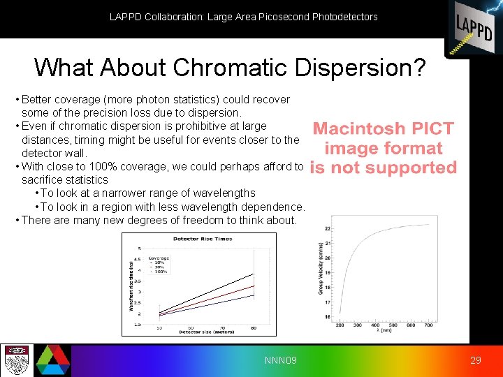
LAPPD Collaboration: Large Area Picosecond Photodetectors What About Chromatic Dispersion? • Better coverage (more photon statistics) could recover some of the precision loss due to dispersion. • Even if chromatic dispersion is prohibitive at large distances, timing might be useful for events closer to the detector wall. • With close to 100% coverage, we could perhaps afford to sacrifice statistics • To look at a narrower range of wavelengths • To look in a region with less wavelength dependence. • There are many new degrees of freedom to think about. NNN 09 29

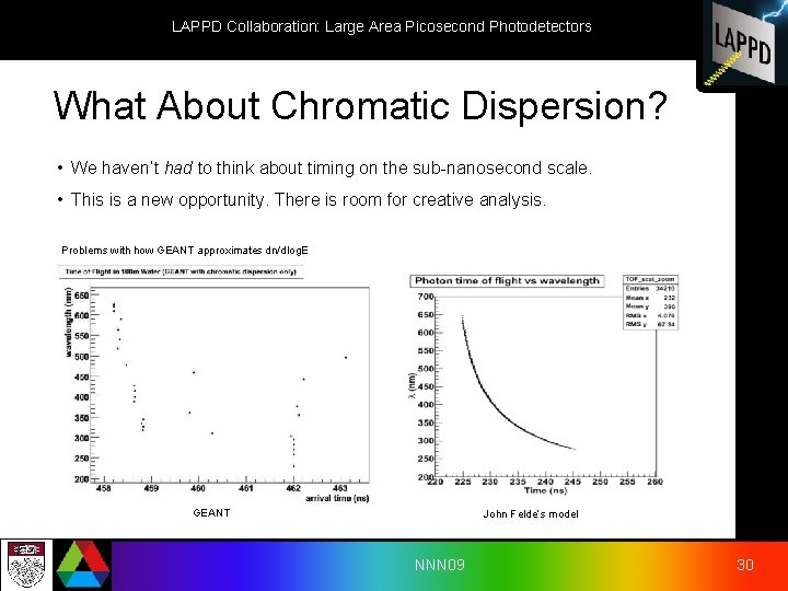
LAPPD Collaboration: Large Area Picosecond Photodetectors What About Chromatic Dispersion? • We haven’t had to think about timing on the sub-nanosecond scale. • This is a new opportunity. There is room for creative analysis. Problems with how GEANT approximates dn/dlog. E GEANT John Felde’s model NNN 09 30