Transmission line design review Theory of lossy line
- Slides: 20

Transmission line design review Theory of lossy line IBM model Bus system Current driver Pre-emphasis 12 March 2021 GTK design review p. jarron NA 62 GTK ASIC 1

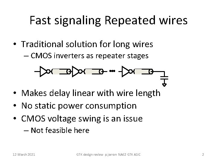
Fast signaling Repeated wires • Traditional solution for long wires – CMOS inverters as repeater stages • Makes delay linear with wire length • No static power consumption • CMOS voltage swing is an issue – Not feasible here 12 March 2021 GTK design review p. jarron NA 62 GTK ASIC 2

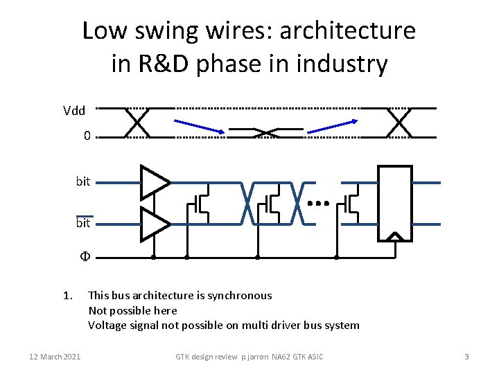
Low swing wires: architecture in R&D phase in industry Vdd 0 bit F 1. 12 March 2021 This bus architecture is synchronous Not possible here Voltage signal not possible on multi driver bus system GTK design review p. jarron NA 62 GTK ASIC 3

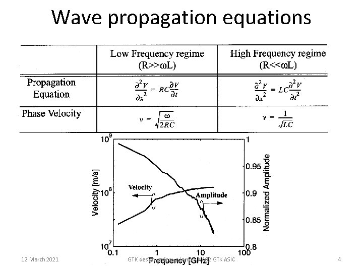
Wave propagation equations 12 March 2021 GTK design review p. jarron NA 62 GTK ASIC 4

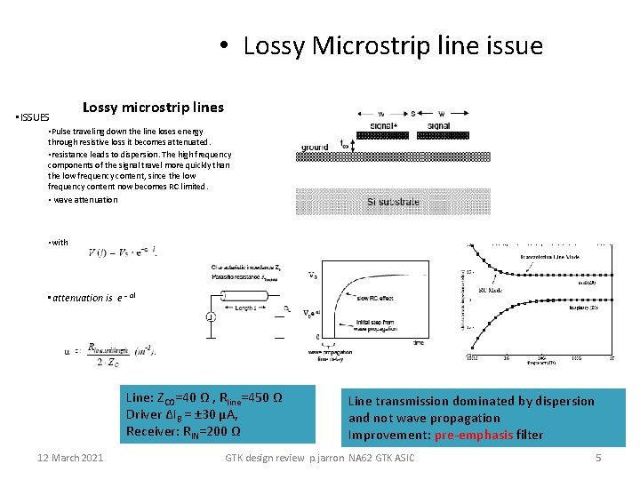
• Lossy Microstrip line issue • ISSUES Lossy microstrip lines • Pulse traveling down the line loses energy through resistive loss it becomes attenuated. • resistance leads to dispersion. The high frequency components of the signal travel more quickly than the low frequency content, since the low frequency content now becomes RC limited. • wave attenuation • with • attenuation is e – αl Line: ZCO=40 Ω , Rline=450 Ω Driver ΔIB = ± 30 µA, Receiver: RIN=200 Ω 12 March 2021 Line transmission dominated by dispersion and not wave propagation Improvement: pre-emphasis filter GTK design review p. jarron NA 62 GTK ASIC 5

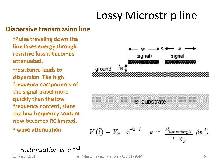
Lossy Microstrip line Dispersive transmission line • Pulse traveling down the line loses energy through resistive loss it becomes attenuated. • resistance leads to dispersion. The high frequency components of the signal travel more quickly than the low frequency content, since the low frequency content now becomes RC limited. • wave attenuation • attenuation is e – αl 12 March 2021 GTK design review p. jarron NA 62 GTK ASIC 6

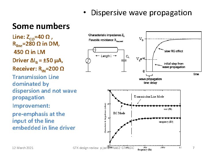
• Dispersive wave propagation Some numbers Line: ZCO=40 Ω , Rline=280 Ω in DM, 450 Ω in LM Driver ΔIB = ± 50 µA, Receiver: RIN=200 Ω Transmission Line dominated by dispersion and not wave propagation Improvement: pre-emphasis at the input of the line embedded in line driver 12 March 2021 GTK design review p. jarron NA 62 GTK ASIC 7

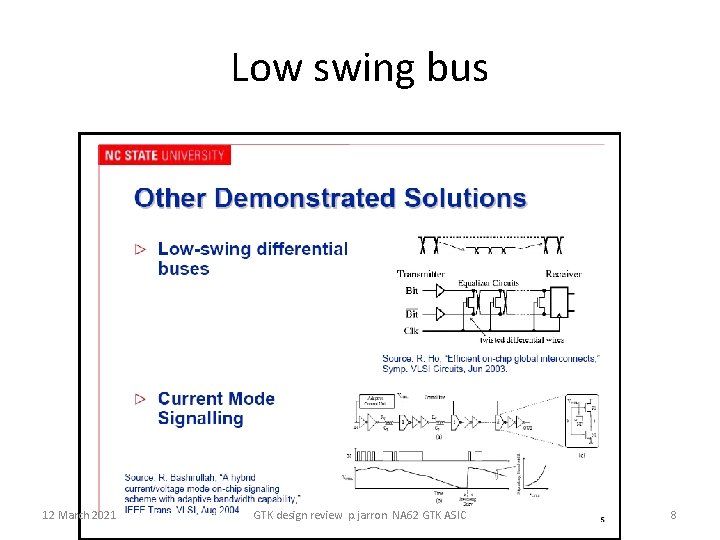
Low swing bus 12 March 2021 GTK design review p. jarron NA 62 GTK ASIC 8

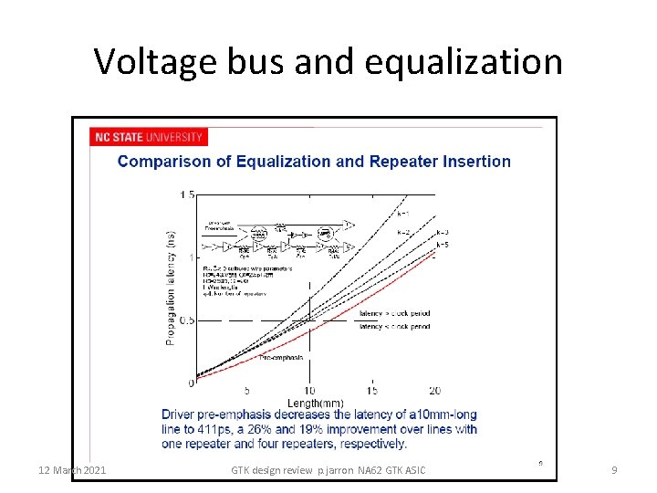
Voltage bus and equalization 12 March 2021 GTK design review p. jarron NA 62 GTK ASIC 9

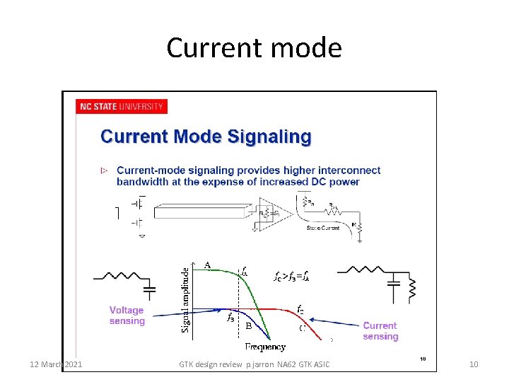
Current mode 12 March 2021 GTK design review p. jarron NA 62 GTK ASIC 10

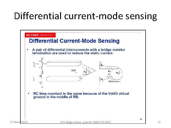
Differential current-mode sensing 12 March 2021 GTK design review p. jarron NA 62 GTK ASIC 11

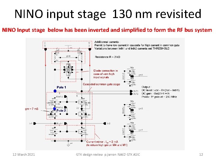
NINO input stage 130 nm revisited NINO Input stage below has been inverted and simplified to form the RF bus system 12 March 2021 GTK design review p. jarron NA 62 GTK ASIC 12

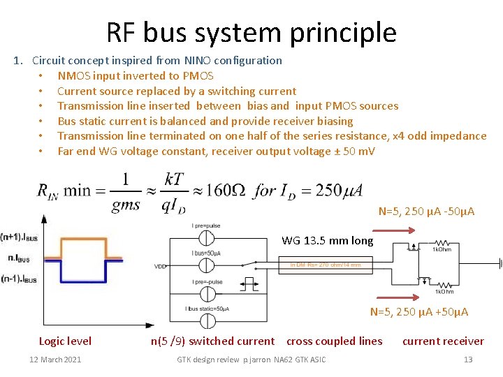
RF bus system principle 1. Circuit concept inspired from NINO configuration • NMOS input inverted to PMOS • Current source replaced by a switching current • Transmission line inserted between bias and input PMOS sources • Bus static current is balanced and provide receiver biasing • Transmission line terminated on one half of the series resistance, x 4 odd impedance • Far end WG voltage constant, receiver output voltage ± 50 m. V N=5, 250 µA -50µA WG 13. 5 mm long N=5, 250 µA +50µA Logic level 12 March 2021 n(5 /9) switched current cross coupled lines GTK design review p. jarron NA 62 GTK ASIC current receiver 13

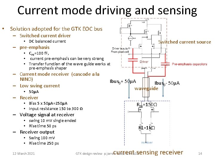
Current mode driving and sensing • Solution adopted for the GTK EOC bus – Switched current driver • DC balanced current Switched current source – pre-emphasis • CPE=100 f. F, • current pre-emphasis can be very strong • Transfer function of the wave guide works at pre-emphasis shaper – Current mode receiver (cascode a la NINO) – Low swing current • 50µA Ibus 0+ 50µA Ibus 0 - 50µA waveguide – Receiver • Bias 5 x 50µA=250µA • Input resistance 150 to 300 Ω RIN=150Ω – Voltage signal at receiver • swing 10 m. V single ended • Rise time 50 ps – Receiver output RL=1 kΩ • Swing 100 m. V • Rise time 250 ps 12 March 2021 current sensing receiver GTK design review p. jarron NA 62 GTK ASIC 14

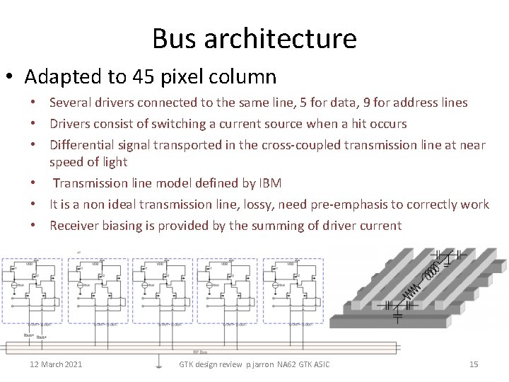
Bus architecture • Adapted to 45 pixel column • Several drivers connected to the same line, 5 for data, 9 for address lines • Drivers consist of switching a current source when a hit occurs • Differential signal transported in the cross-coupled transmission line at near speed of light • Transmission line model defined by IBM • It is a non ideal transmission line, lossy, need pre-emphasis to correctly work • Receiver biasing is provided by the summing of driver current 12 March 2021 GTK design review p. jarron NA 62 GTK ASIC 15

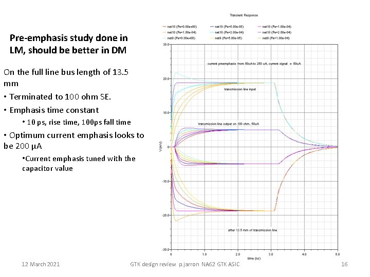
Pre-emphasis study done in LM, should be better in DM On the full line bus length of 13. 5 mm • Terminated to 100 ohm SE. • Emphasis time constant • 10 ps, rise time, 100 ps fall time • Optimum current emphasis looks to be 200 µA • Current emphasis tuned with the capacitor value 12 March 2021 GTK design review p. jarron NA 62 GTK ASIC 16

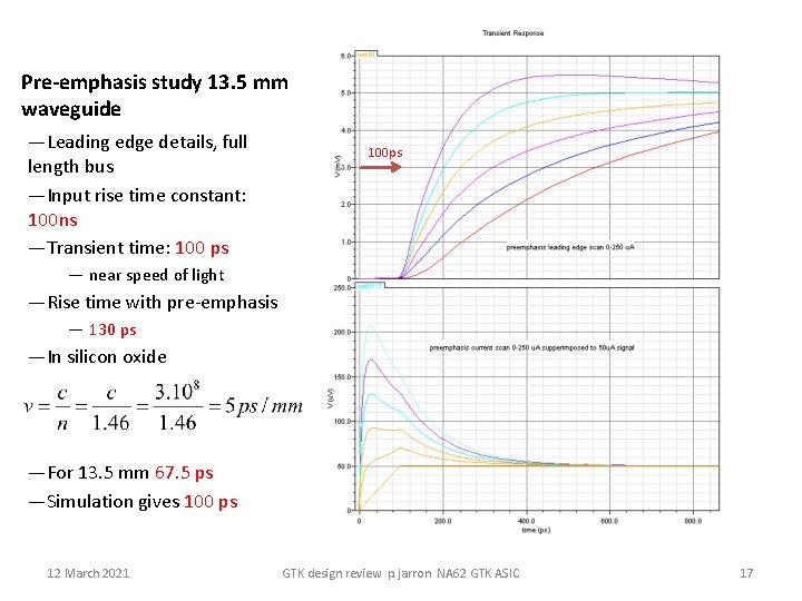
Pre-emphasis study 13. 5 mm waveguide —Leading edge details, full length bus —Input rise time constant: 100 ns —Transient time: 100 ps 100 ps — near speed of light —Rise time with pre-emphasis — 130 ps —In silicon oxide —For 13. 5 mm 67. 5 ps —Simulation gives 100 ps 12 March 2021 GTK design review p. jarron NA 62 GTK ASIC 17

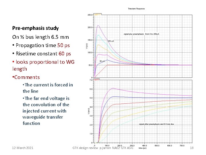
Pre-emphasis study On ½ bus length 6. 5 mm • Propagation time 50 ps • Risetime constant 60 ps • looks proportional to WG length • Comments • The current is forced in the line • The far end voltage is the convolution of the injected current with waveguide transfer function 12 March 2021 GTK design review p. jarron NA 62 GTK ASIC 18

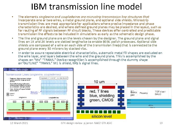
IBM transmission line model • • • The elements singlewire and coupledwires are microstrip transmission line structures that incorporate one or two wires, a metal ground plane, and optional side shields. Microstrip transmission lines are most appropriate for applications where precise impedance and phase characteristics are desired, and where defined ground planes may be placed in the layout, such as for routing of RF signals between RF circuit blocks. These devices offer controlled and predictable transmission line effects to be included in simulations as early as the schematic design phase. The line and ground plane are on the levels chosen by the designer. The ground plane and signal lines on 1 X and 2 X levels are slotted lengthwise to enable BEOL polish processes. Optional side shields are composed of a wire on each side of the transmission line(s) that is connected to the ground plane every 50 microns by stacked vias. In order to assure repeatable electrical characteristics, automatic metal fill shapes are excluded on the wire layer, and layers between the wire and the ground plane. This is accomplished by the shapes on “Mx” “TRANS. ” Device recognition is accomplished through the dummy shape on“OUTLINE” “TRANS. ” M 1 is shield, MQ is signal lines. 12 March 2021 GTK design review p. jarron NA 62 GTK ASIC 19

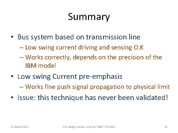
Summary • Bus system based on transmission line – Low swing current driving and sensing O. K – Works correctly, depends on the precision of the IBM model • Low swing Current pre-emphasis – Works fine push signal propagation to physical limit • Issue: this technique has never been validated! 12 March 2021 GTK design review p. jarron NA 62 GTK ASIC 20