Thermal Transport in Nano Electronics Jungwan Cho Ph
- Slides: 10
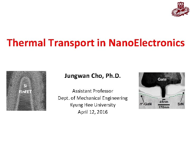
Thermal Transport in Nano. Electronics Jungwan Cho, Ph. D. Si Fin. FET Assistant Professor Dept. of Mechanical Engineering Kyung Hee University April 12, 2016
Short Bio Jungwan Cho (조정완) jungwan. cho@khu. ac. kr Assistant Professor Department of Mechanical Engineering, Kyung Hee Univ. Education June 2010—Sep. 2014 Sep. 2008—June 2010 Mar. 2001—Feb. 2008 Ph. D. in Mechanical Engineering, Stanford University M. S. in Mechanical Engineering, Stanford University B. S. in Mechanical Engineering, Seoul National University Professional Experience Oct. 2014—Feb. 2016 Postdoctoral Research Associate Department of Mechanical Engineering, Stanford Univ. Research Interests Micro- and nanoscale heat conduction/ Experimental characterization of thermal properties (ultrafast optical methods)/ Electronics cooling/ Energy conversion 2
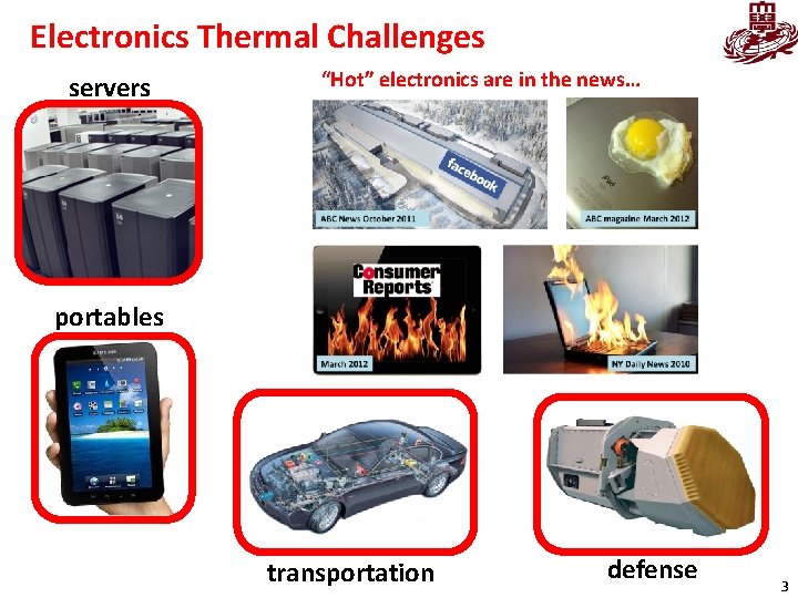
Electronics Thermal Challenges servers “Hot” electronics are in the news… portables transportation defense 3
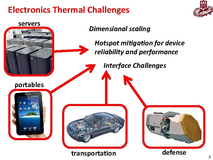
Electronics Thermal Challenges servers Dimensional scaling Hotspot mitigation for device reliability and performance Interface Challenges portables transportation defense 3
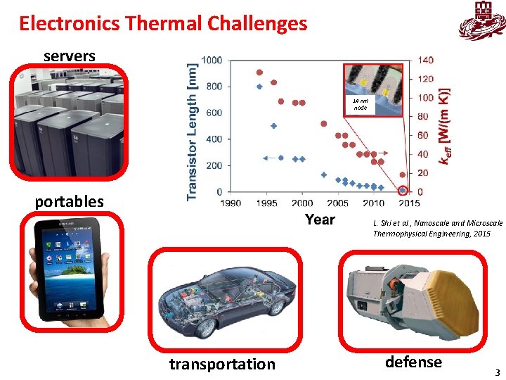
Electronics Thermal Challenges servers 14 nm node portables L. Shi et al. , Nanoscale and Microscale Thermophysical Engineering, 2015 transportation defense 3
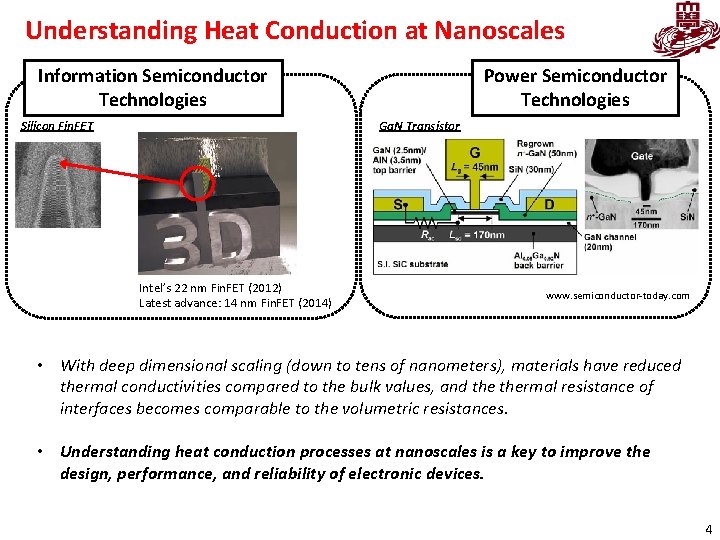
Understanding Heat Conduction at Nanoscales Power Semiconductor Technologies Information Semiconductor Technologies Silicon Fin. FET Ga. N Transistor Intel’s 22 nm Fin. FET (2012) Latest advance: 14 nm Fin. FET (2014) www. semiconductor-today. com • With deep dimensional scaling (down to tens of nanometers), materials have reduced thermal conductivities compared to the bulk values, and thermal resistance of interfaces becomes comparable to the volumetric resistances. • Understanding heat conduction processes at nanoscales is a key to improve the design, performance, and reliability of electronic devices. 4
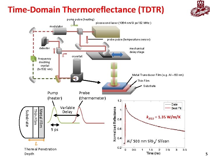
Time-Domain Thermoreflectance (TDTR) pump pulse (heating) picosecond laser (1064 nm/ 9 ps/ 82 MHz ) modulator probe pulse (temperature sensor) detector mechanical delay stage cryostat frequency doubling crystal (to 532 nm) Metal Transducer Film (e. g. Al – 60 nm) Thin Film Substrate Pump (heater) Metal Film Thin Film Substrate Variable Delay Probe (thermometer) k. Si. O 2 = 1. 35 W/m/K 9 ps Thermal Penetration Depth Al/ 500 nm Si. O 2/ Silicon 5
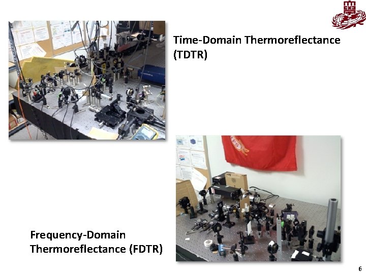
Time-Domain Thermoreflectance (TDTR) Frequency-Domain Thermoreflectance (FDTR) 6
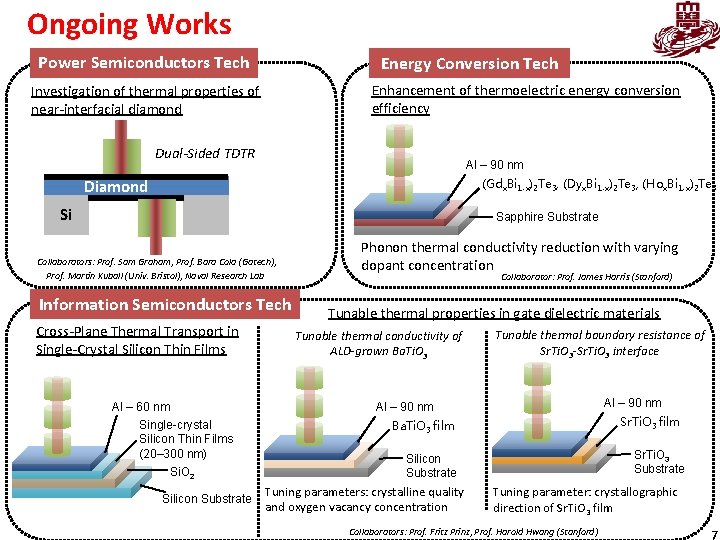
Ongoing Works Power Semiconductors Tech Energy Conversion Tech Enhancement of thermoelectric energy conversion efficiency Investigation of thermal properties of near-interfacial diamond Dual-Sided TDTR Al – 90 nm (Gdx. Bi 1 -x)2 Te 3, (Dyx. Bi 1 -x)2 Te 3, (Hox. Bi 1 -x)2 Te 3 Diamond Si Sapphire Substrate Collaborators: Prof. Sam Graham, Prof. Bara Cola (Gatech), Prof. Martin Kuball (Univ. Bristol), Naval Research Lab Information Semiconductors Tech Cross-Plane Thermal Transport in Single-Crystal Silicon Thin Films Phonon thermal conductivity reduction with varying dopant concentration Collaborator: Prof. James Harris (Stanford) Tunable thermal properties in gate dielectric materials Tunable thermal conductivity of ALD-grown Ba. Ti. O 3 Tunable thermal boundary resistance of Sr. Ti. O 3 -Sr. Ti. O 3 interface Al – 90 nm Al – 60 nm Single-crystal Silicon Thin Films (20– 300 nm) Si. O 2 Silicon Substrate Sr. Ti. O 3 film Ba. Ti. O 3 film Sr. Ti. O 3 Substrate Silicon Substrate Tuning parameters: crystalline quality and oxygen vacancy concentration Tuning parameter: crystallographic direction of Sr. Ti. O 3 film Collaborators: Prof. Fritz Prinz, Prof. Harold Hwang (Stanford) 7
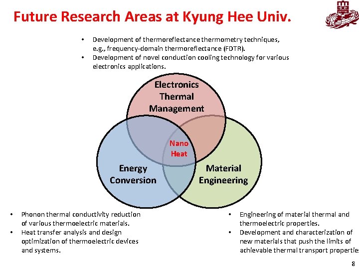
Future Research Areas at Kyung Hee Univ. • • Development of thermoreflectance thermometry techniques, e. g. , frequency-domain thermoreflectance (FDTR). Development of novel conduction cooling technology for various electronics applications. Electronics Thermal Management Nano Heat Energy Conversion • • Phonon thermal conductivity reduction of various thermoelectric materials. Heat transfer analysis and design optimization of thermoelectric devices and systems. Material Engineering • • Engineering of material thermal and thermoelectric properties. Development and characterization of new materials that push the limits of achievable thermal transport properties 8