Surface Emissions Pole Piece etc SE 3 Xrays


 PMMA")


")


 • NEC monitor: 380 x 300 mm; 1280 x 1024 pixels.")


sqrt(Ip/ β) –")
- Slides: 24
Surface Emissions Pole Piece, etc SE 3 X-rays Cathodoluminescence l ≈ 1 nm for metals up to 10 nm for insulator Specimen current
Dependence of backscatter coefficient on backscattered electron energy
Backscattering increases strongly with Z independent of beam energy
Backscatter dependence on tilt and Z
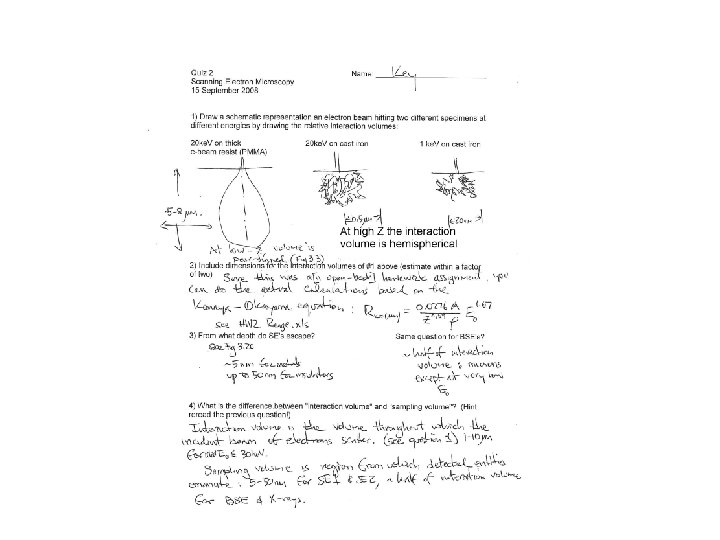
Where are electrons coming from? • Kanaya – Okayama equation for electron range in a material: • Rk-o = (0. 0276 A E 01. 67)/(Z 0. 89ρ) μm – For E 0 in ke. V, ρ in gm/cm 3, A in gm/mole and Z = atomic number
Where are electrons coming from? Material A Z ρ E 0 R (μm) PMMA 12. 01 6 1. 16 20 8. 63295 Fe 55. 26 26 7. 87 20 1. 58759 Fe 55. 26 26 7. 87 Homework 2. 2 1 0. 01066
Depth of origination of backscattered electrons Backscattered electrons can Investigate deep into the sample
Distribution of scattered electron energies Note that the distinction between SE and BSE is a definition There are only “scattered electrons”
Why do backscattered electrons give the most information about chemical composition ? Why don’t secondary electrons give much information about chemical composition?
Dependence of scattered electron yield on Z 50%! Nearly independent 10%
Why do secondary electrons give great topographic information?
Image formation and interpretation
Image formation and interpretation Images from exactly the same area of the sample taken with different detectors.
In case you thought the second image was just taken at higher contrast…
And it’s not just your detector choice that can impact your image… 20 k. V 500 V
Everhart. Thornley detector (1960)
Scanning and Data Collection
Transfer of image from sample to screen Works for both topographic and elemental information
Pixels (Picture elements) • NEC monitor: 380 x 300 mm; 1280 x 1024 pixels. Hence pixel size on monitor size is 297 x 293 microns. . . 300 microns. • Typical file size used in FEI Nova Nano. SEM is 1024 x 884 pixels. • Pixel size on sample is pixel size on monitor divided by magnification, about 15 microns (20 X) to 0. 6 nm (500 k. X).
So what; who cares? • Example: 10 ke. V beam at 100 p. A viewing at 100 X (neural array was taken at 118 X) saved into 1024 x 884 file using Leo and FEI. • β = 4 Ip/π2αp 2 dp 2 • dp = (2 WD/πr. A)sqrt(Ip/ β) • FEI: dp = (2*5 mm/π*. 015 mm)sqrt(10 -10 Acm 2 sr/108 A) = 0. 5 nm! • Leo: (2*8 mm/π*. 01 mm)sqrt(10 -10 A cm 2 sr/105 A) = 40 nm!
So what; who cares? Cont’d • So – Your pixel size varies from 0. 6 nm to 15 microns – Your beam diameter can vary from 0. 5 nm to 40 microns, at the smallest – Your interaction volume varies from 10 microns to 10 nm (BSE, SE 2; last homework)
Implications • If probe size is too small – You are wasting resolution: topography can change between sampling points (Nyquist Theorem!) – Resolution regained by sampling and saving more points – You are wasting signal to noise – You are wasting contrast
How to make the spot larger? • dp = (2 WD/πr. A)sqrt(Ip/ β) – Increase working distance – Go to a smaller aperture – Increase probe current – Decrease accelerating potential • Is this the dominant effect of decreasing the accelerating potential?