SPICE SPICE Simulation Program with Integrated Circuit Emphasis



- Slides: 14

SPICE

SPICE (Simulation Program with Integrated Circuit Emphasis) is a general-purpose, open source , analog electronic circuit simulator. It is a powerful program that is used in integrated circuits and board-level design to check the integrity of circuit designs and to predict circuit behavior.

NEED for SPICE �Simulating the circuit with SPICE is the industrystandard way to verify circuit operation at the transistor level before committing to manufacturing an integrated circuit. �Even with a breadboard, some circuit properties may not be accurate compared to the final printed wiring board, such as parasitic resistances and capacitances. These parasitic components can often be estimated more accurately using SPICE simulation.

SPICE for MOSFETS n Three Built in MODELS : n. LEVEL 1 : Described by Square Law V/I characteristics. n LEVEL 2: Detailed analytical MOSFET model n LEVEL 3: It is a semi Empirical model.

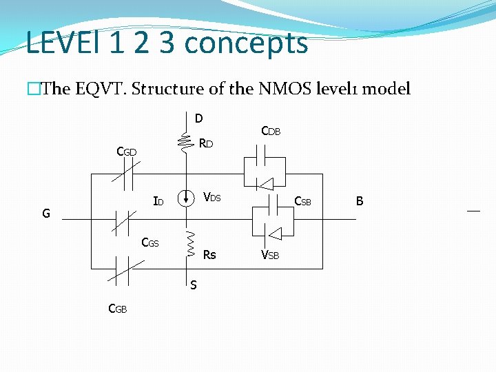
LEVEl 1 2 3 concepts �The EQVT. Structure of the NMOS level 1 model D RD CGD VDS ID G CGS Rs S CGB CDB CSB VSB B

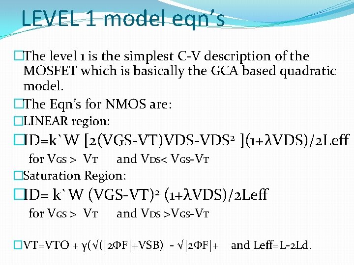
LEVEL 1 model eqn’s �The level 1 is the simplest C-V description of the MOSFET which is basically the GCA based quadratic model. �The Eqn’s for NMOS are: �LINEAR region: �ID=k`W [2(VGS-VT)VDS-VDS 2 ](1+λVDS)/2 Leff for VGS > VT and VDS< VGS-VT �Saturation Region: �ID= k`W (VGS-VT)2 (1+λVDS)/2 Leff for VGS > VT and VDS >VGS-VT �VT=VTO + γ(√(|2ΦF|+VSB) - √|2ΦF|+ and Leff=L-2 Ld.

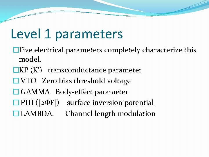
Level 1 parameters �Five electrical parameters completely characterize this model. �KP (K’) transconductance parameter � VTO Zero bias threshold voltage � GAMMA Body-effect parameter � PHI (|2ΦF|) surface inversion potential � LAMBDA. Channel length modulation

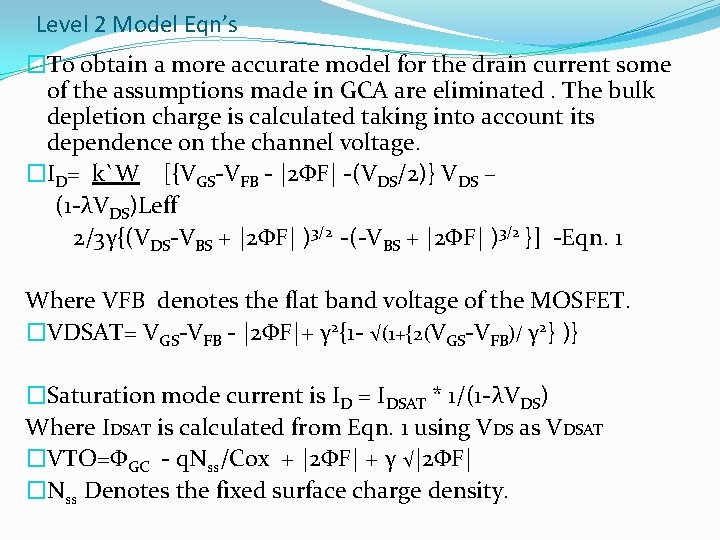
Level 2 Model Eqn’s �To obtain a more accurate model for the drain current some of the assumptions made in GCA are eliminated. The bulk depletion charge is calculated taking into account its dependence on the channel voltage. �ID= k`W [{VGS-VFB - |2ΦF| -(VDS/2)} VDS – (1 -λVDS)Leff 2/3γ{(VDS-VBS + |2ΦF| )3/2 -(-VBS + |2ΦF| )3/2 }] -Eqn. 1 Where VFB denotes the flat band voltage of the MOSFET. �VDSAT= VGS-VFB - |2ΦF|+ γ 2{1 - √(1+{2(VGS-VFB)/ γ 2} )} �Saturation mode current is ID = IDSAT * 1/(1 -λVDS) Where IDSAT is calculated from Eqn. 1 using VDS as VDSAT �VTO=ΦGC - q. Nss/Cox + |2ΦF| + γ √|2ΦF| �Nss Denotes the fixed surface charge density.

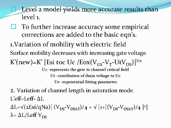
� Level 2 model yields more accurate results than level 1. � To further increase accuracy some empirical corrections are added to the basic eqn’s. 1. Variation of mobility with electric field Surface mobility decreases with increasing gate voltage. K’(new)=K’ [Esi toc Uc /Eox(VGS-VT-Ut. VDS)]Ue Uc -represents the gate to channel critical field Ut -contibution of drain voltage to Uc Ue -exponential fitting parameter. 2. Variation of channel length in saturation mode. L’eff=Leff- ∆L ∆L=√(2 Esi/q. Na)[ (VDS-VDSAT)/4 + √ [1+[(VDS-VDSAT)/4 ]2] λ= ∆L/Leff VDS

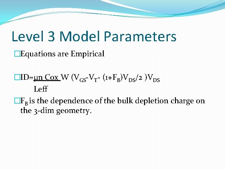
Level 3 Model Parameters �Equations are Empirical �ID=µn Cox W (VGS-VT- (1+FB)VDS/2 )VDS Leff �FB is the dependence of the bulk depletion charge on the 3 -dim geometry.

Comparison of the MOSFET Models �Level 1 model is not very precise because the GCA used in the derivation is approximate and no of fitting parameters is too small. �Level 2 requires a larger amount of CPU time for calculation if all parameters are added �Level 3 has the disadvantage of difficulty in calculating some of its parameters �Level 1 is useful for a quick and rough estimate of the circuit performance without much accuracy �Level 2 can be used with differing complexities by adding the parameters that this model supports �Level 3 achieves the same level of accuracy as level 2 but CPU time is less and no of iterations are less.

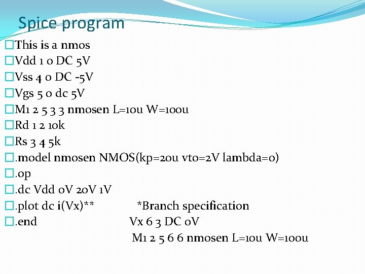
Spice program �This is a nmos �Vdd 1 0 DC 5 V �Vss 4 0 DC -5 V �Vgs 5 0 dc 5 V �M 1 2 5 3 3 nmosen L=10 u W=100 u �Rd 1 2 10 k �Rs 3 4 5 k �. model nmosen NMOS(kp=20 u vto=2 V lambda=0) �. op �. dc Vdd 0 V 20 V 1 V �. plot dc i(Vx)** *Branch specification �. end Vx 6 3 DC 0 V M 1 2 5 6 6 nmosen L=10 u W=100 u

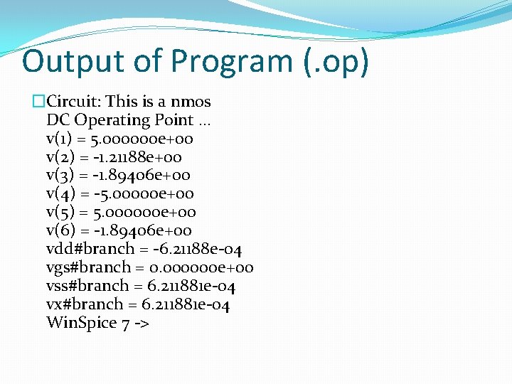
Output of Program (. op) �Circuit: This is a nmos DC Operating Point. . . v(1) = 5. 000000 e+00 v(2) = -1. 21188 e+00 v(3) = -1. 89406 e+00 v(4) = -5. 00000 e+00 v(5) = 5. 000000 e+00 v(6) = -1. 89406 e+00 vdd#branch = -6. 21188 e-04 vgs#branch = 0. 000000 e+00 vss#branch = 6. 211881 e-04 vx#branch = 6. 211881 e-04 Win. Spice 7 ->

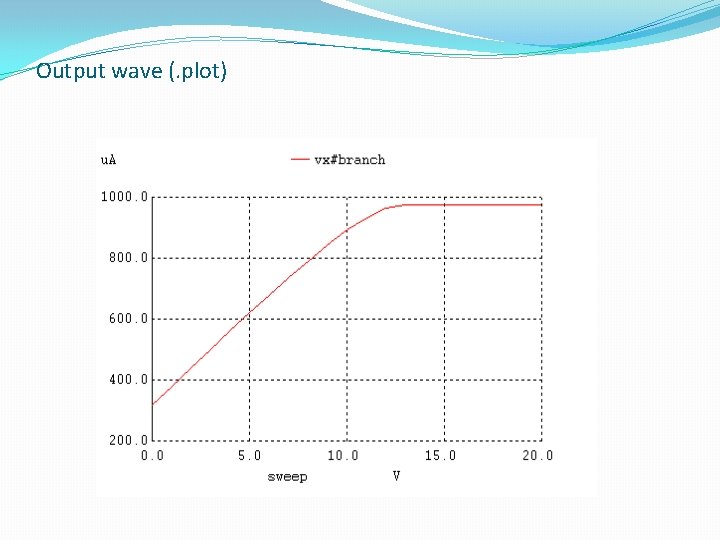
Output wave (. plot)