INTRODUCTION Spice SPICE Simulation Program with Integrated Circuit




- Slides: 65

INTRODUCTION Spice

SPICE Simulation Program with Integrated Circuit Emphasis

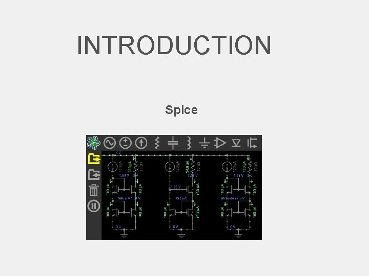
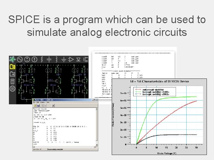
SPICE is a program which can be used to simulate analog electronic circuits

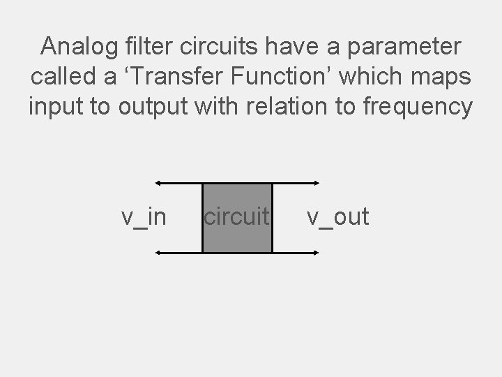
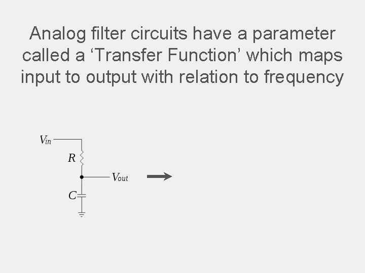
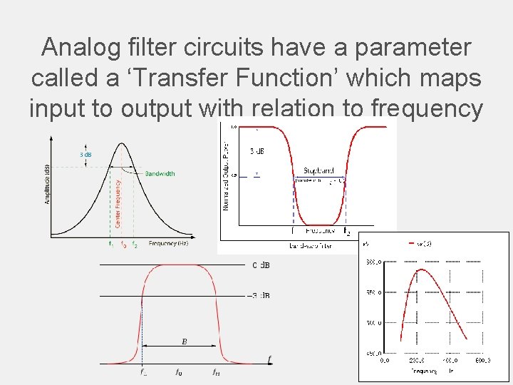
Analog filter circuits have a parameter called a ‘Transfer Function’ which maps input to output with relation to frequency v_in circuit v_out

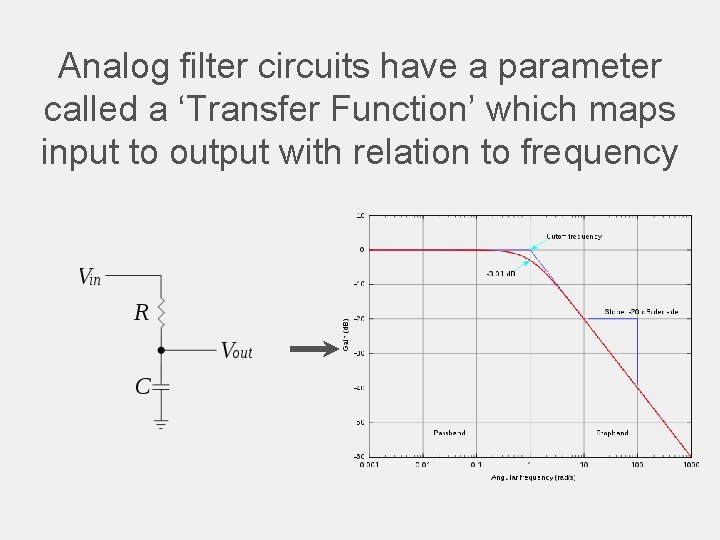
Analog filter circuits have a parameter called a ‘Transfer Function’ which maps input to output with relation to frequency

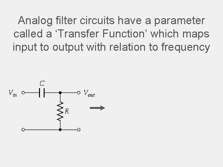
Analog filter circuits have a parameter called a ‘Transfer Function’ which maps input to output with relation to frequency

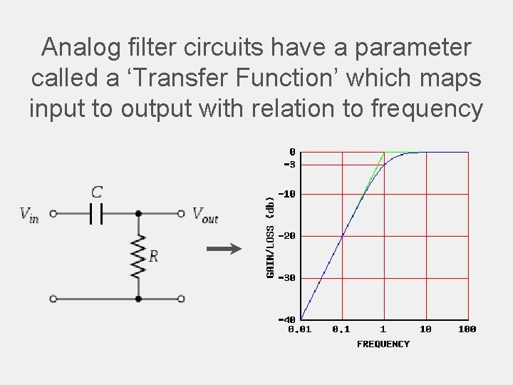
Analog filter circuits have a parameter called a ‘Transfer Function’ which maps input to output with relation to frequency

Analog filter circuits have a parameter called a ‘Transfer Function’ which maps input to output with relation to frequency

Analog filter circuits have a parameter called a ‘Transfer Function’ which maps input to output with relation to frequency

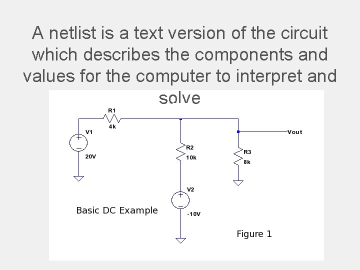
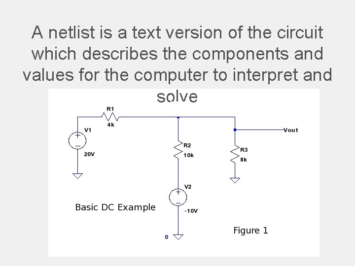
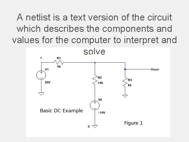
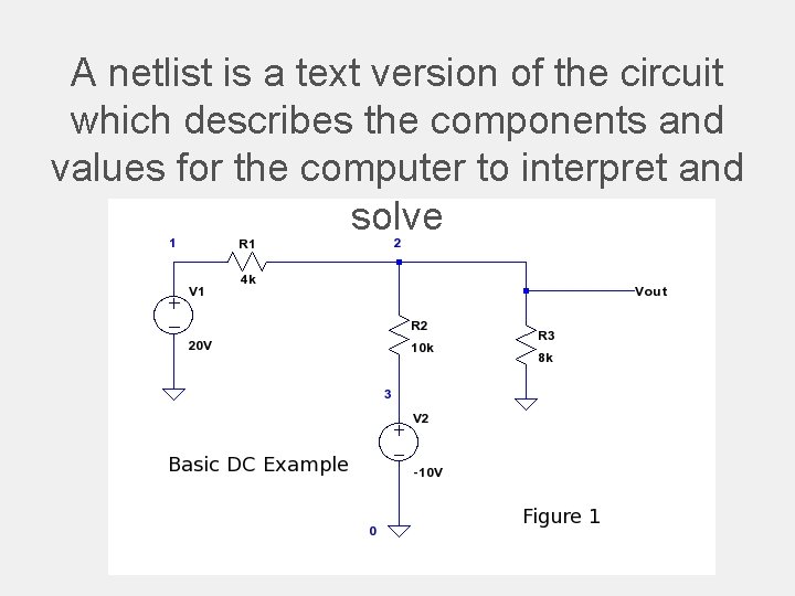
A netlist is a text version of the circuit which describes the components and values for the computer to interpret and solve

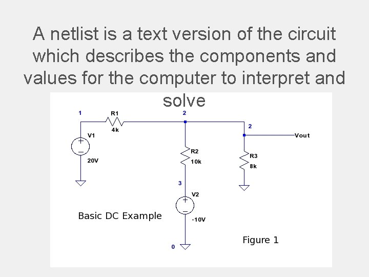
A netlist is a text version of the circuit which describes the components and values for the computer to interpret and solve

A netlist is a text version of the circuit which describes the components and values for the computer to interpret and solve

A netlist is a text version of the circuit which describes the components and values for the computer to interpret and solve

A netlist is a text version of the circuit which describes the components and values for the computer to interpret and solve

A netlist is a text version of the circuit which describes the components and values for the computer to interpret and solve

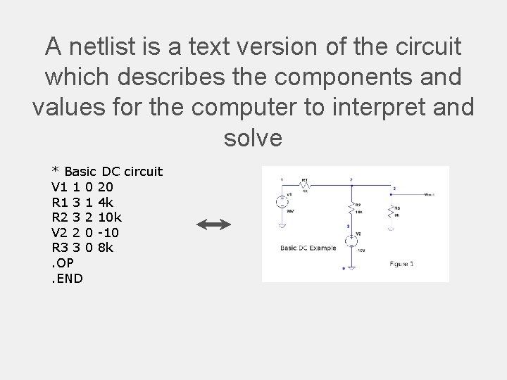
A netlist is a text version of the circuit which describes the components and values for the computer to interpret and solve * Basic DC circuit V 1 1 0 20 R 1 3 1 4 k R 2 3 2 10 k V 2 2 0 -10 R 3 3 0 8 k. OP. END

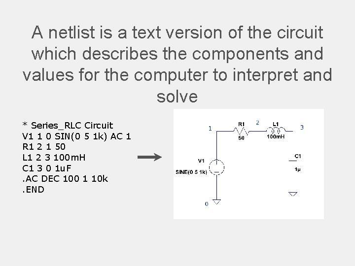
A netlist is a text version of the circuit which describes the components and values for the computer to interpret and solve * Series_RLC Circuit V 1 1 0 SIN(0 5 1 k) AC 1 R 1 2 1 50 L 1 2 3 100 m. H C 1 3 0 1 u. F. AC DEC 100 1 10 k. END

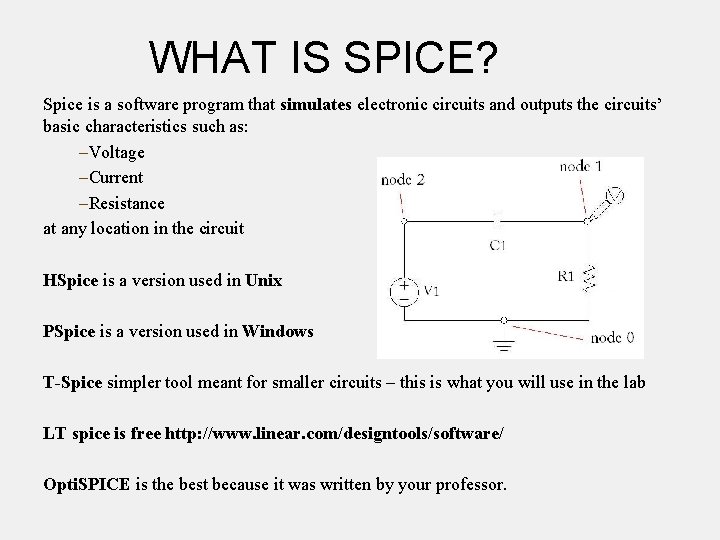
WHAT IS SPICE? Spice is a software program that simulates electronic circuits and outputs the circuits’ basic characteristics such as: –Voltage –Current –Resistance at any location in the circuit HSpice is a version used in Unix PSpice is a version used in Windows T-Spice simpler tool meant for smaller circuits – this is what you will use in the lab LT spice is free http: //www. linear. com/designtools/software/ Opti. SPICE is the best because it was written by your professor.

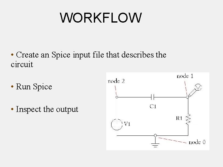
WORKFLOW • Create an Spice input file that describes the circuit • Run Spice • Inspect the output

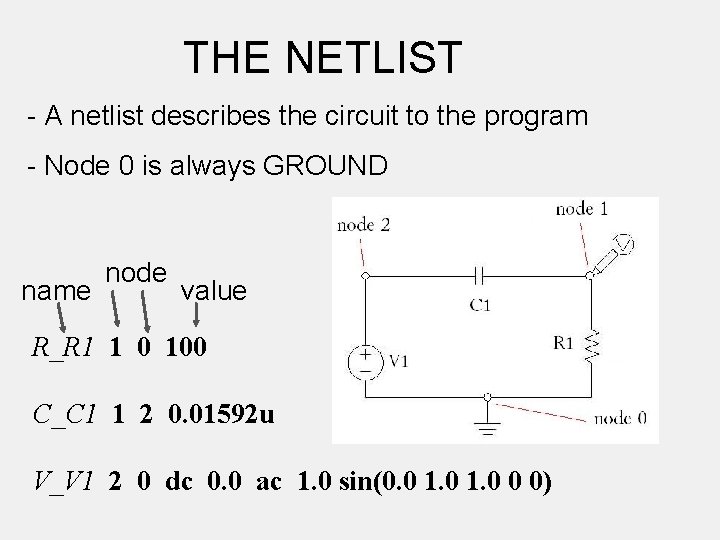
THE NETLIST - A netlist describes the circuit to the program - Node 0 is always GROUND name node value R_R 1 1 0 100 C_C 1 1 2 0. 01592 u V_V 1 2 0 dc 0. 0 ac 1. 0 sin(0. 0 1. 0 0 0)

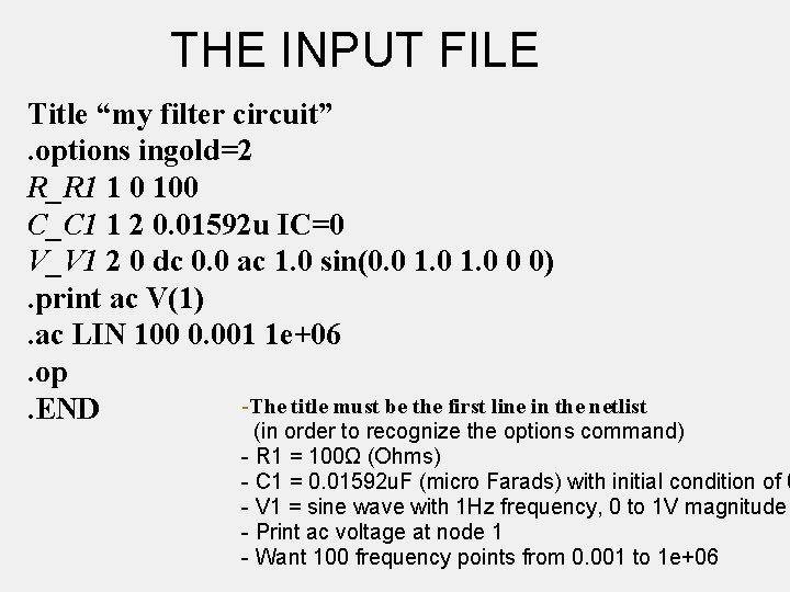
THE INPUT FILE Title “my filter circuit”. options ingold=2 R_R 1 1 0 100 C_C 1 1 2 0. 01592 u IC=0 V_V 1 2 0 dc 0. 0 ac 1. 0 sin(0. 0 1. 0 0 0). print ac V(1). ac LIN 100 0. 001 1 e+06. op -The title must be the first line in the netlist. END (in order to recognize the options command) - R 1 = 100Ω (Ohms) - C 1 = 0. 01592 u. F (micro Farads) with initial condition of 0 - V 1 = sine wave with 1 Hz frequency, 0 to 1 V magnitude - Print ac voltage at node 1 - Want 100 frequency points from 0. 001 to 1 e+06

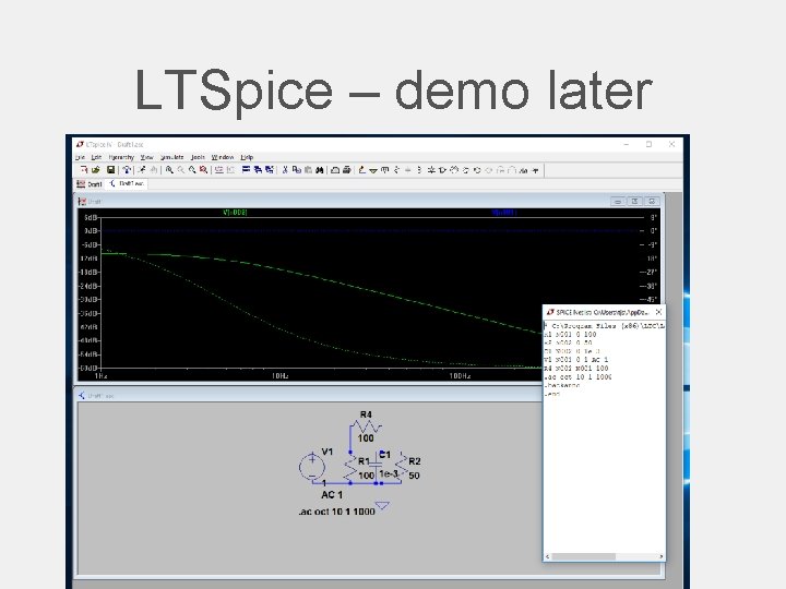
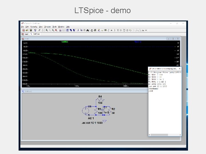
LTSpice – demo later

Others might be available • Hspice (not likely and difficult to use) • Instructions likely obsolete • PSpice • Not sure we have full licence • Tspice • Might be ok – netlist based I think. • Opti. Spice – the best (it’s mine).

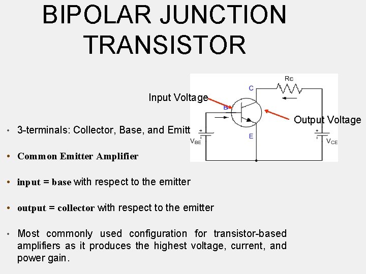
BIPOLAR JUNCTION TRANSISTOR Input Voltage • 3 -terminals: Collector, Base, and Emitter • Common Emitter Amplifier • input = base with respect to the emitter • output = collector with respect to the emitter • Most commonly used configuration for transistor-based amplifiers as it produces the highest voltage, current, and power gain. Output Voltage

BJT

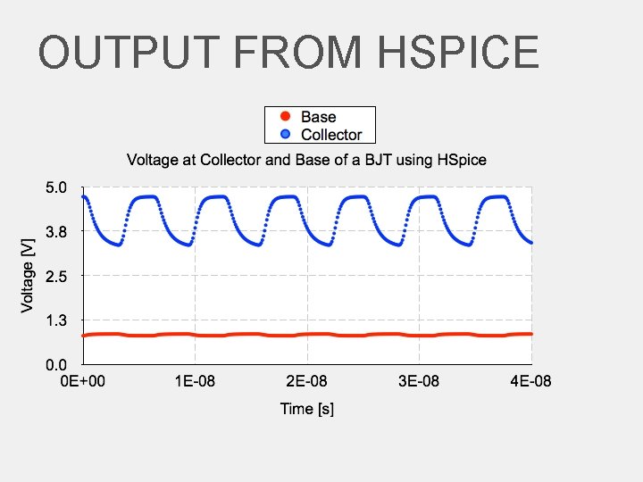
OUTPUT FROM HSPICE

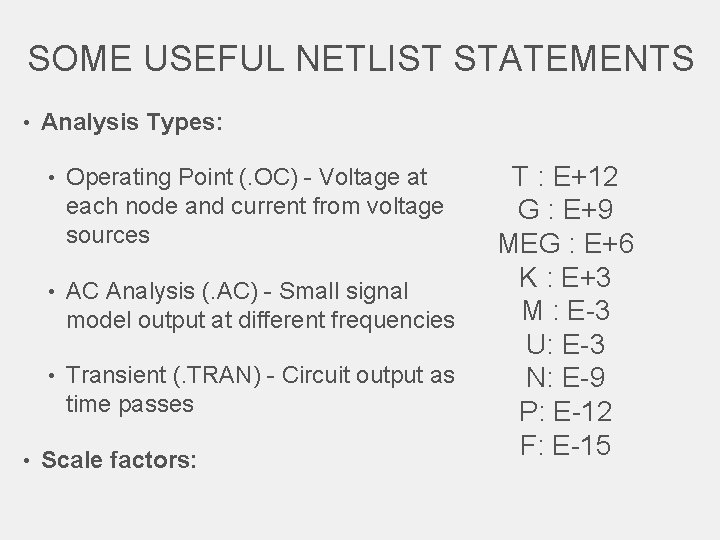
SOME USEFUL NETLIST STATEMENTS • Analysis Types: • Operating Point (. OC) - Voltage at each node and current from voltage sources • AC Analysis (. AC) - Small signal model output at different frequencies • Transient (. TRAN) - Circuit output as time passes • Scale factors: T : E+12 G : E+9 MEG : E+6 K : E+3 M : E-3 U: E-3 N: E-9 P: E-12 F: E-15

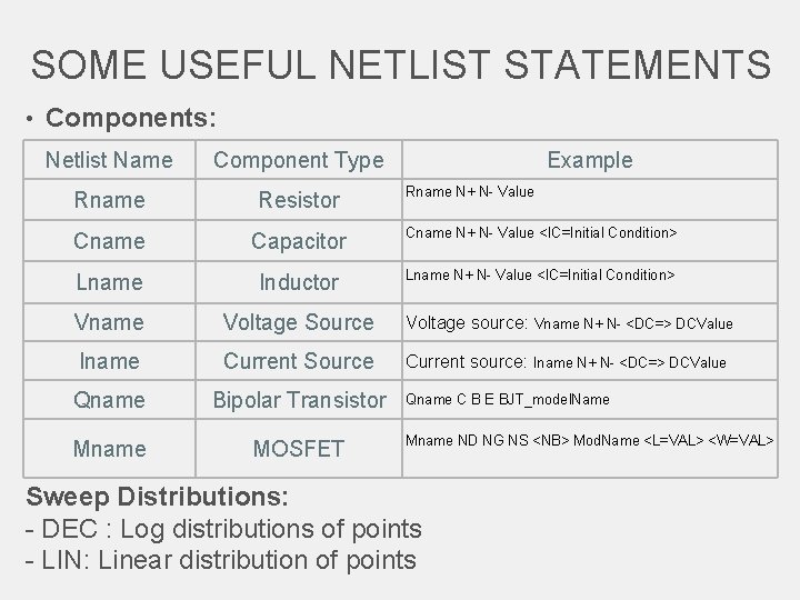
SOME USEFUL NETLIST STATEMENTS • Components: Netlist Name Component Type Example Rname Resistor Cname Capacitor Cname N+ N- Value <IC=Initial Condition> Lname Inductor Lname N+ N- Value <IC=Initial Condition> Vname Voltage Source Voltage source: Vname N+ N- <DC=> DCValue Iname Current Source Current source: Iname N+ N- <DC=> DCValue Qname Bipolar Transistor Mname MOSFET Rname N+ N- Value Qname C B E BJT_model. Name Mname ND NG NS <NB> Mod. Name <L=VAL> <W=VAL> Sweep Distributions: - DEC : Log distributions of points - LIN: Linear distribution of points

LTSpice - demo

Electronics Principles & Applications 8 th Edition Charles A. Schuler LTspice IV Mc. Graw-Hill © 2013 by The Mc. Graw-Hill Companies, Inc. All rights reserved

LTspice IV is a free download and can be found on the Linear Technology website: http: //www. linear. com/designtools/software/switchercad. jsp

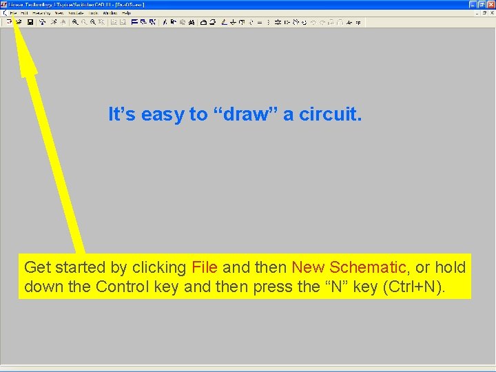
It’s easy to “draw” a circuit. Get started by clicking File and then New Schematic, or hold down the Control key and then press the “N” key (Ctrl+N).

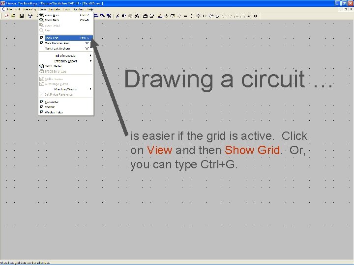
Drawing a circuit … is easier if the grid is active. Click on View and then Show Grid. Or, you can type Ctrl+G.

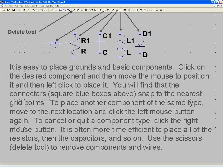
Delete tool It is easy to place grounds and basic components. Click on the desired component and then move the mouse to position it and then left click to place it. You will find that the connectors (square blue boxes above) snap to the nearest grid points. To place another component of the same type, move to the next location and click the left mouse button again. To cancel or quit a component type, click the right mouse button. It is often more time efficient to place all of the resistors, then the capacitors, and so on. Use the scissors (delete tool) to remove components and wires.

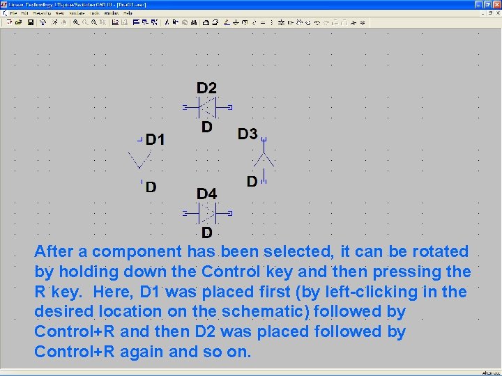
After a component has been selected, it can be rotated by holding down the Control key and then pressing the R key. Here, D 1 was placed first (by left-clicking in the desired location on the schematic) followed by Control+R and then D 2 was placed followed by Control+R again and so on.

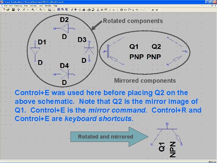
Rotated components Mirrored components Control+E was used here before placing Q 2 on the above schematic. Note that Q 2 is the mirror image of Q 1. Control+E is the mirror command. Control+R and Control+E are keyboard shortcuts. Rotated and mirrored

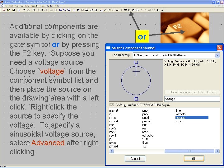
Additional components are available by clicking on the gate symbol or by pressing the F 2 key. Suppose you need a voltage source. Choose “voltage” from the component symbol list and then place the source on the drawing area with a left click. Right click the source to specify the voltage. To specify a sinusoidal voltage source, select Advanced after right clicking. or

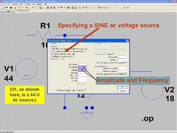
Specifying a SINE ac voltage source Amplitude and Frequency (V 1, as shown here, is a 44 -V dc source. )

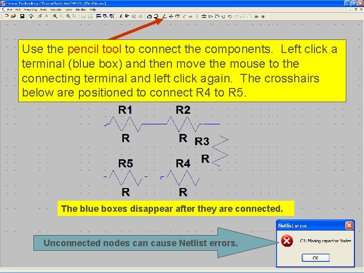
Use the pencil tool to connect the components. Left click a terminal (blue box) and then move the mouse to the connecting terminal and left click again. The crosshairs below are positioned to connect R 4 to R 5. The blue boxes disappear after they are connected. Unconnected nodes can cause Netlist errors.

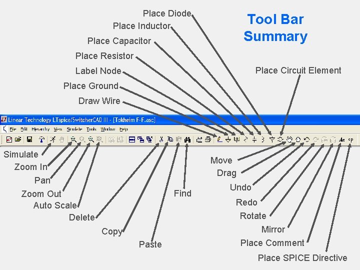
Place Diode Place Inductor Tool Bar Summary Place Capacitor Place Resistor Place Circuit Element Label Node Place Ground Draw Wire Simulate Zoom In Pan Move Drag Find Zoom Out Auto Scale Delete Undo Redo Rotate Mirror Copy Paste Place Comment Place SPICE Directive

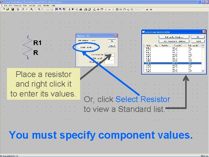
Place a resistor and right click it to enter its values. Or, click Select Resistor to view a Standard list. You must specify component values.

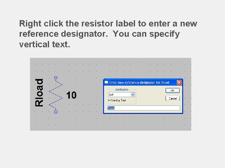
Right click the resistor label to enter a new reference designator. You can specify vertical text.

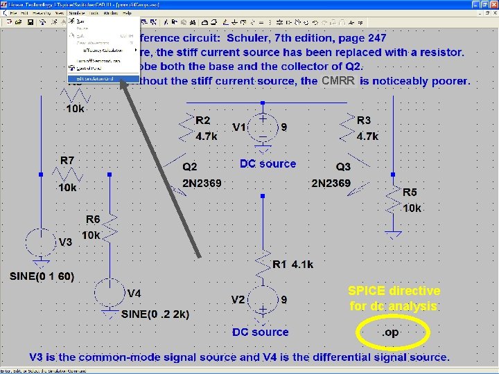
CMRR SPICE directive for dc analysis

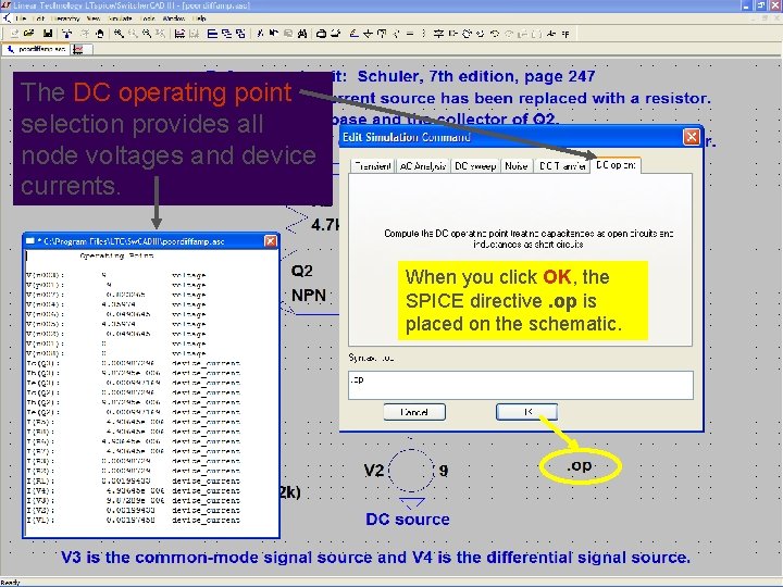
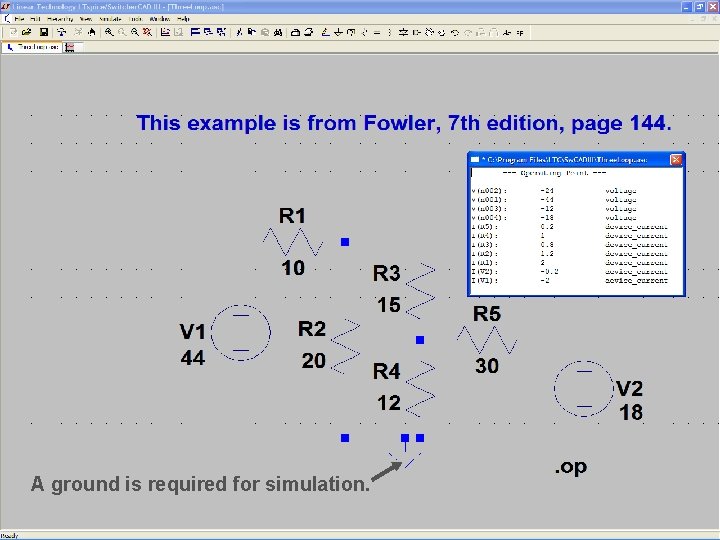
The DC operating point selection provides all node voltages and device currents. When you click OK, the SPICE directive. op is placed on the schematic.

A ground is required for simulation.

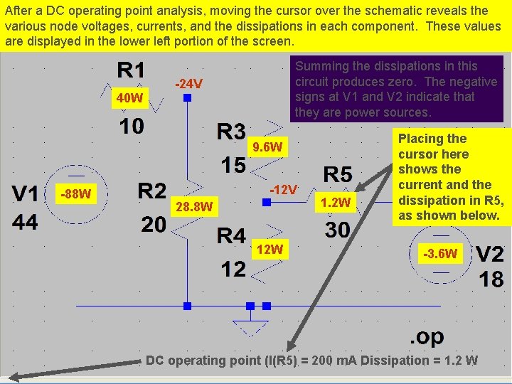
After a DC operating point analysis, moving the cursor over the schematic reveals the various node voltages, currents, and the dissipations in each component. These values are displayed in the lower left portion of the screen. Summing the dissipations in this circuit produces zero. The negative signs at V 1 and V 2 indicate that they are power sources. -24 V 40 W 9. 6 W -88 W -12 V 28. 8 W 12 W 1. 2 W Placing the cursor here shows the current and the dissipation in R 5, as shown below. -3. 6 W DC operating point (I(R 5) = 200 m. A Dissipation = 1. 2 W

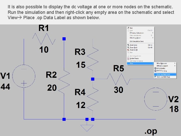
It is also possible to display the dc voltage at one or more nodes on the schematic. Run the simulation and then right-click any empty area on the schematic and select View Place. op Data Label as shown below.

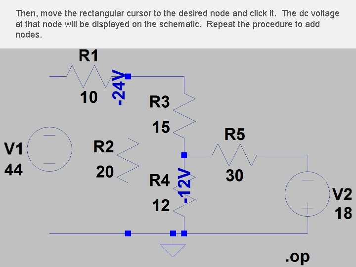
Then, move the rectangular cursor to the desired node and click it. The dc voltage at that node will be displayed on the schematic. Repeat the procedure to add nodes.

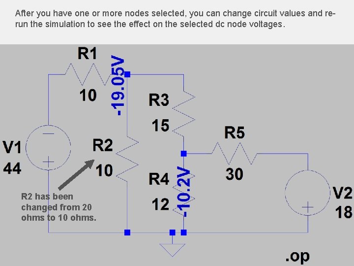
After you have one or more nodes selected, you can change circuit values and rerun the simulation to see the effect on the selected dc node voltages. R 2 has been changed from 20 ohms to 10 ohms.

Waveforms are what one sees on an oscilloscope (graphs of instantaneous voltages versus time). Waveforms can be viewed via the transient analysis option. Click on Simulate, Edit Sim Command, and then select the Transient tab. The next three slides show the procedure.

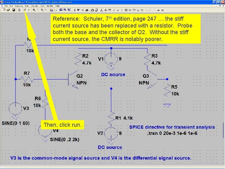
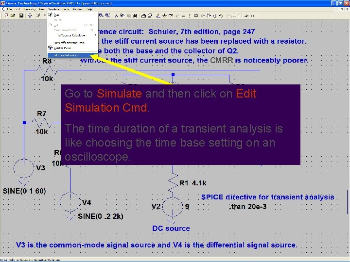
Reference: Schuler, 7 th edition, page 247 … the stiff current source has been replaced with a resistor. Probe both the base and the collector of Q 2. Without the stiff current source, the CMRR is notably poorer. Load the circuit from the file menu. Then, click run.

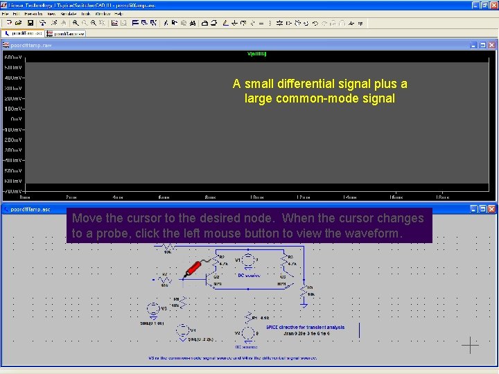
A small differential signal plus a large common-mode signal Move the cursor to the desired node. When the cursor changes to a probe, click the left mouse button to view the waveform.

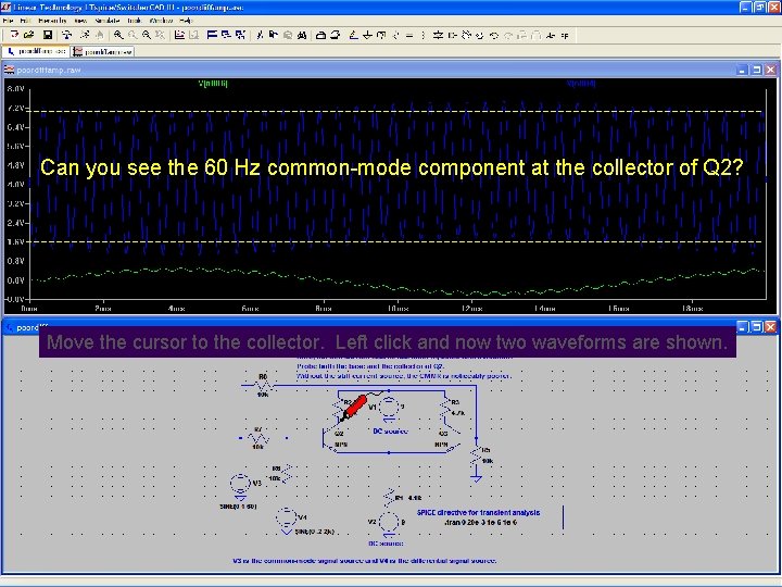
Can you see the 60 Hz common-mode component at the collector of Q 2? Move the cursor to the collector. Left click and now two waveforms are shown.

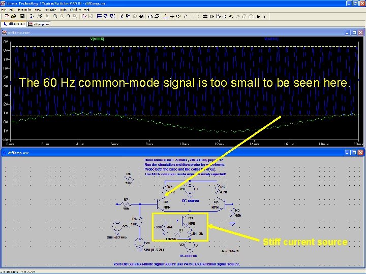
The next slide demonstrates the value of simulation when evaluating circuit performance. The differential amplifier circuit is much improved with a stiff current source. The common-mode rejection ratio (CMRR) is remarkably better. The common mode signal cannot be seen in the output. Circuit simulators make it easy and fun to investigate issues such as this.

The 60 Hz common-mode signal is too small to be seen here. Stiff current source

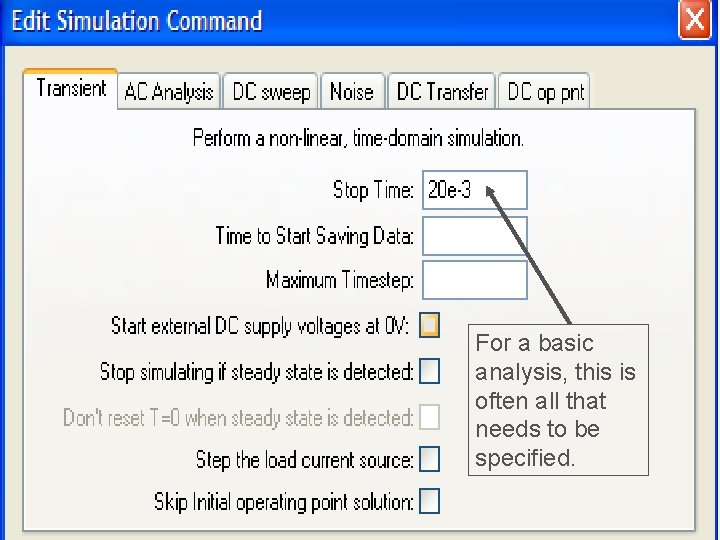
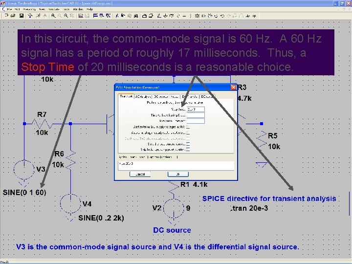
Remember, waveforms are available via transient analysis. You must specify the time duration of a transient analysis by specifying a Stop Time. Often, this is all that is required. You can also specify the Time to Start Saving Data. Useful in circuits where the start-up period is not important. You can also specify the Maximum Timestep.

CMRR Go to Simulate and then click on Edit Simulation Cmd. The time duration of a transient analysis is like choosing the time base setting on an oscilloscope.

For a basic analysis, this is often all that needs to be specified.

In this circuit, the common-mode signal is 60 Hz. A 60 Hz signal has a period of roughly 17 milliseconds. Thus, a Stop Time of 20 milliseconds is a reasonable choice.

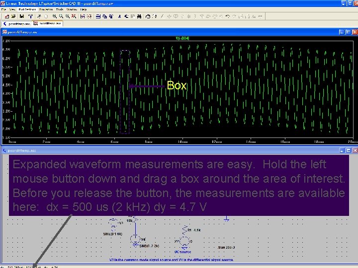
Box Expanded waveform measurements are easy. Hold the left mouse button down and drag a box around the area of interest. Before you release the button, the measurements are available here: dx = 500 us (2 k. Hz) dy = 4. 7 V

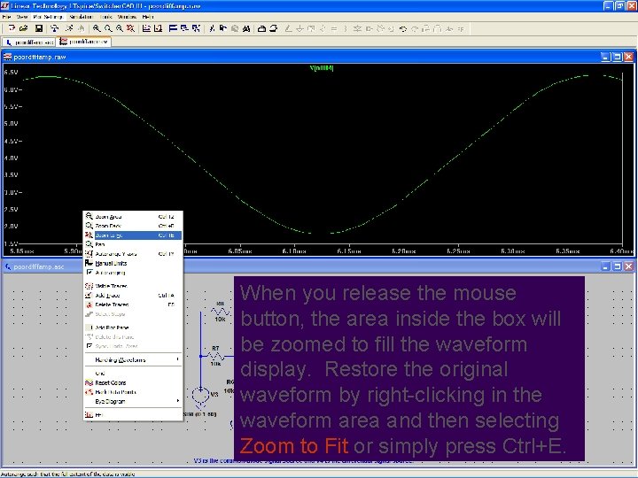
When you release the mouse button, the area inside the box will be zoomed to fill the waveform display. Restore the original waveform by right-clicking in the waveform area and then selecting Zoom to Fit or simply press Ctrl+E.

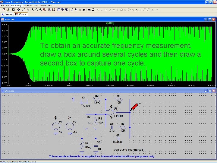
To obtain an accurate frequency measurement, draw a box around several cycles and then draw a second box to capture one cycle.

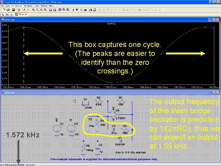
This box captures one cycle. (The peaks are easier to identify than the zero crossings. ) 1. 572 k. Hz The output frequency of this Wien bridge oscillator is predicted by 1/(2πRC), thus we can expect an output at 1. 59 k. Hz.

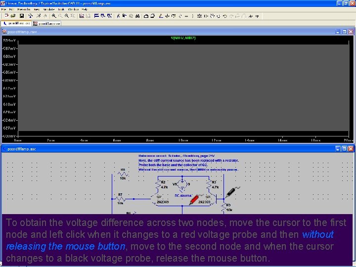
To obtain the voltage difference across two nodes, move the cursor to the first node and left click when it changes to a red voltage probe and then without releasing the mouse button, move to the second node and when the cursor changes to a black voltage probe, release the mouse button.

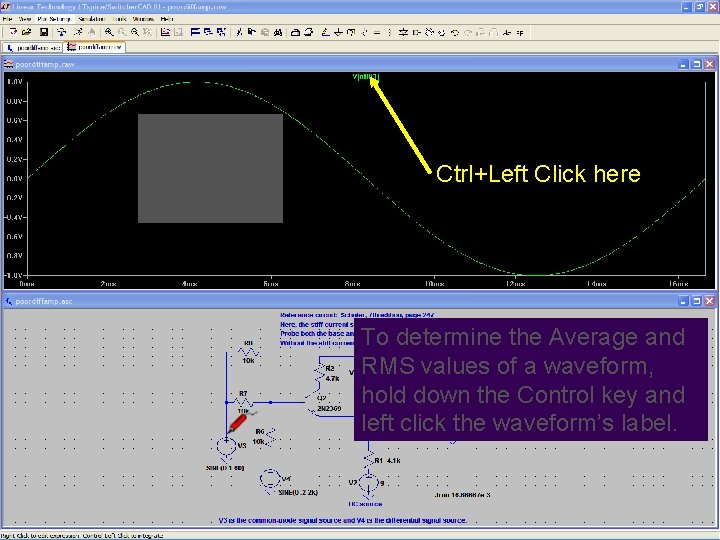
Ctrl+Left Click here To determine the Average and RMS values of a waveform, hold down the Control key and left click the waveform’s label.