Filters and Tuned Amplifiers 1 Figure 12 1

- Slides: 64

Filters and Tuned Amplifiers 1

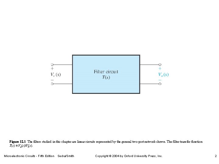
Figure 12. 1 The filters studied in this chapter are linear circuits represented by the general two-port network shown. The filter transfer function T(s) º Vo(s)/Vi(s). Microelectronic Circuits - Fifth Edition Sedra/Smith Copyright 2004 by Oxford University Press, Inc. 2

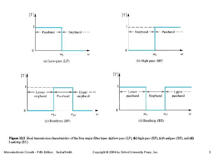
Figure 12. 2 Ideal transmission characteristics of the four major filter types: (a) low-pass (LP), (b) high-pass (HP), (c) bandpass (BP), and (d) bandstop (BS). Microelectronic Circuits - Fifth Edition Sedra/Smith Copyright 2004 by Oxford University Press, Inc. 3

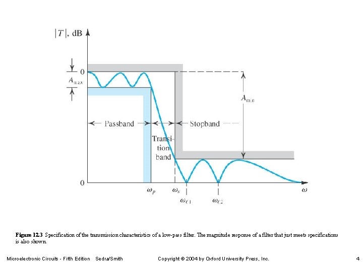
Figure 12. 3 Specification of the transmission characteristics of a low-pass filter. The magnitude response of a filter that just meets specifications is also shown. Microelectronic Circuits - Fifth Edition Sedra/Smith Copyright 2004 by Oxford University Press, Inc. 4

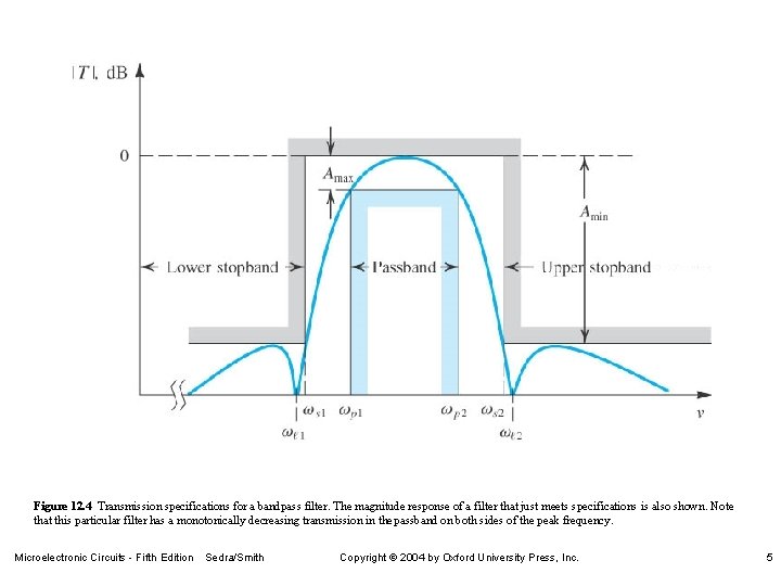
Figure 12. 4 Transmission specifications for a bandpass filter. The magnitude response of a filter that just meets specifications is also shown. Note that this particular filter has a monotonically decreasing transmission in the passband on both sides of the peak frequency. Microelectronic Circuits - Fifth Edition Sedra/Smith Copyright 2004 by Oxford University Press, Inc. 5

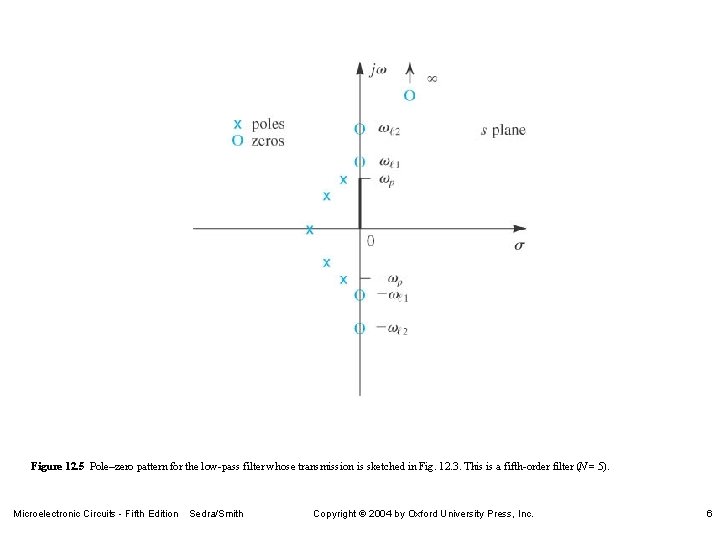
Figure 12. 5 Pole–zero pattern for the low-pass filter whose transmission is sketched in Fig. 12. 3. This is a fifth-order filter (N = 5). Microelectronic Circuits - Fifth Edition Sedra/Smith Copyright 2004 by Oxford University Press, Inc. 6

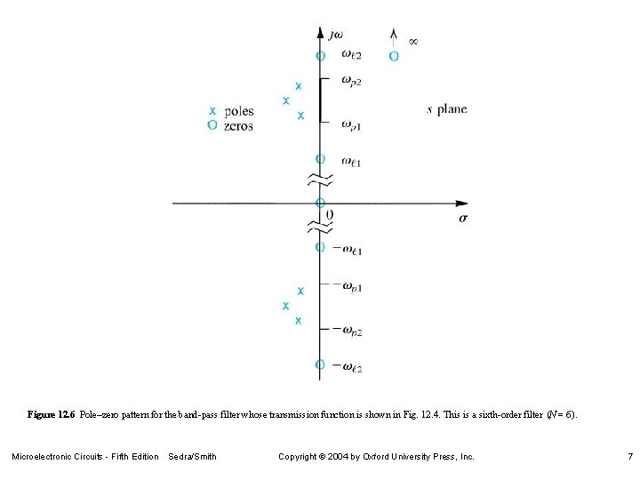
Figure 12. 6 Pole–zero pattern for the band-pass filter whose transmission function is shown in Fig. 12. 4. This is a sixth-order filter (N = 6). Microelectronic Circuits - Fifth Edition Sedra/Smith Copyright 2004 by Oxford University Press, Inc. 7

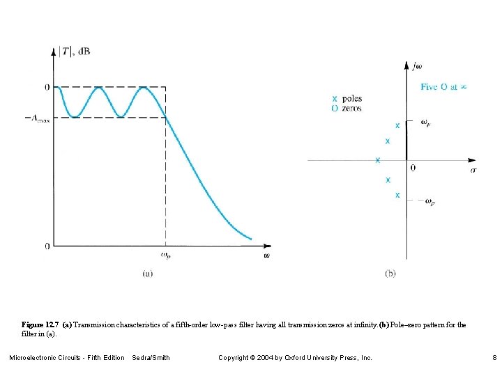
Figure 12. 7 (a) Transmission characteristics of a fifth-order low-pass filter having all transmission zeros at infinity. (b) Pole–zero pattern for the filter in (a). Microelectronic Circuits - Fifth Edition Sedra/Smith Copyright 2004 by Oxford University Press, Inc. 8

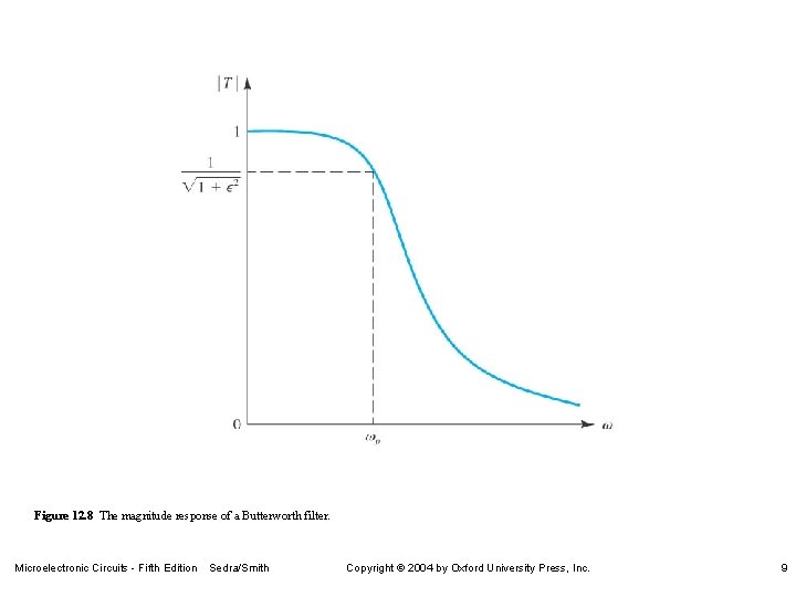
Figure 12. 8 The magnitude response of a Butterworth filter. Microelectronic Circuits - Fifth Edition Sedra/Smith Copyright 2004 by Oxford University Press, Inc. 9

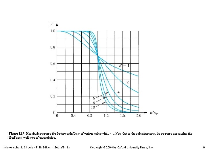
Figure 12. 9 Magnitude response for Butterworth filters of various order with e = 1. Note that as the order increases, the response approaches the ideal brick-wall type of transmission. Microelectronic Circuits - Fifth Edition Sedra/Smith Copyright 2004 by Oxford University Press, Inc. 10

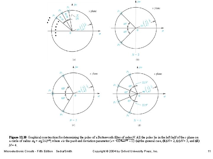
Figure 12. 10 Graphical construction for determining the poles of a Butterworth filter of order N. All the poles lie in the left half of the s plane on a circle of radius w 0 = wp(1/e)1/N, where e is the passband deviation parameter (e = Ö 10 Amax/10 – 1): (a) the general case, (b) N = 2, (c) N = 3, and (d) N = 4. Microelectronic Circuits - Fifth Edition Sedra/Smith Copyright 2004 by Oxford University Press, Inc. 11

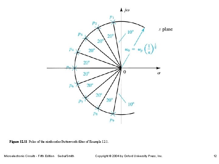
Figure 12. 11 Poles of the ninth-order Butterworth filter of Example 12. 1. Microelectronic Circuits - Fifth Edition Sedra/Smith Copyright 2004 by Oxford University Press, Inc. 12

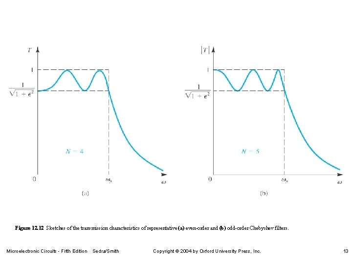
Figure 12. 12 Sketches of the transmission characteristics of representative (a) even-order and (b) odd-order Chebyshev filters. Microelectronic Circuits - Fifth Edition Sedra/Smith Copyright 2004 by Oxford University Press, Inc. 13

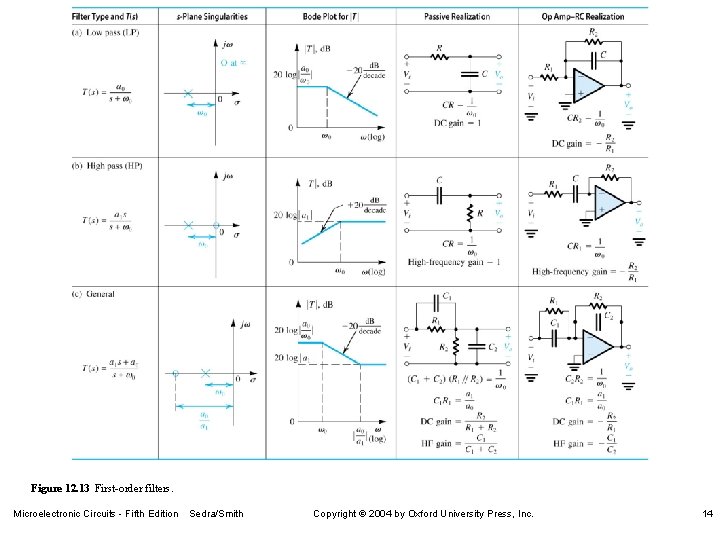
Figure 12. 13 First-order filters. Microelectronic Circuits - Fifth Edition Sedra/Smith Copyright 2004 by Oxford University Press, Inc. 14

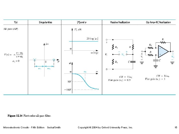
Figure 12. 14 First-order all-pass filter. Microelectronic Circuits - Fifth Edition Sedra/Smith Copyright 2004 by Oxford University Press, Inc. 15

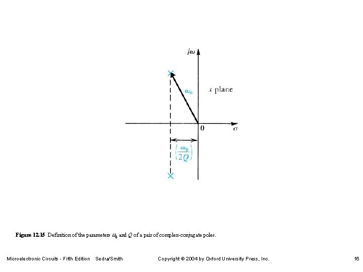
Figure 12. 15 Definition of the parameters w 0 and Q of a pair of complex-conjugate poles. Microelectronic Circuits - Fifth Edition Sedra/Smith Copyright 2004 by Oxford University Press, Inc. 16

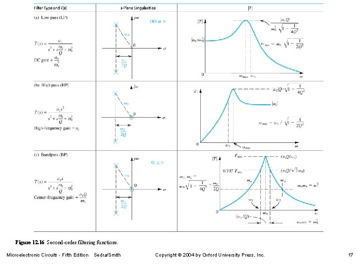
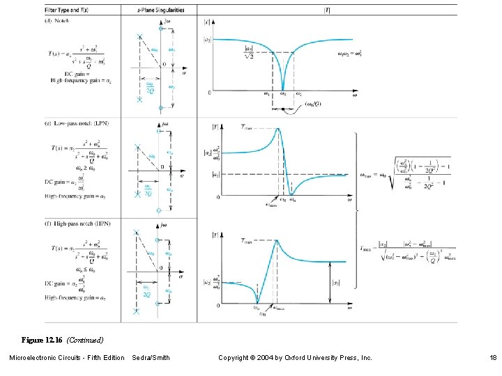
Figure 12. 16 Second-order filtering functions. Microelectronic Circuits - Fifth Edition Sedra/Smith Copyright 2004 by Oxford University Press, Inc. 17

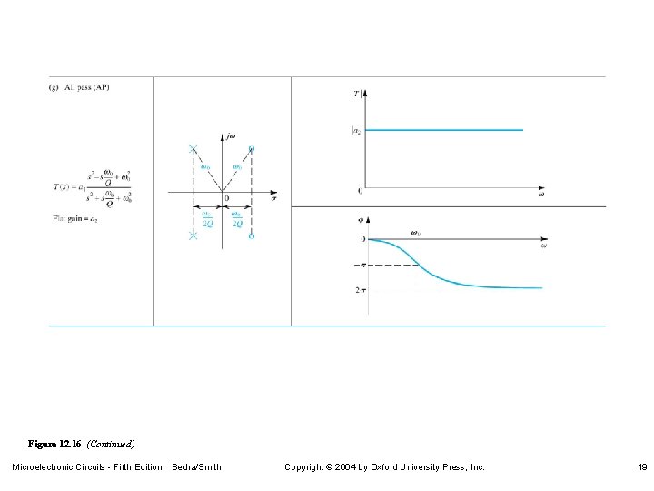
Figure 12. 16 (Continued) Microelectronic Circuits - Fifth Edition Sedra/Smith Copyright 2004 by Oxford University Press, Inc. 18

Figure 12. 16 (Continued) Microelectronic Circuits - Fifth Edition Sedra/Smith Copyright 2004 by Oxford University Press, Inc. 19

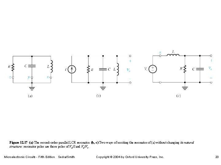
Figure 12. 17 (a) The second-order parallel LCR resonator. (b, c) Two ways of exciting the resonator of (a) without changing its natural structure: resonator poles are those poles of Vo/I and Vo/Vi. Microelectronic Circuits - Fifth Edition Sedra/Smith Copyright 2004 by Oxford University Press, Inc. 20

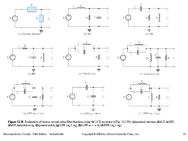
Figure 12. 18 Realization of various second-order filter functions using the LCR resonator of Fig. 12. 17(b): (a) general structure, (b) LP, (c) HP, (d) BP, (e) notch at w 0, (f) general notch, (g) LPN (wn ³ w 0), (h) LPN as s ® ¥, (i) HPN (wn < w 0). Microelectronic Circuits - Fifth Edition Sedra/Smith Copyright 2004 by Oxford University Press, Inc. 21

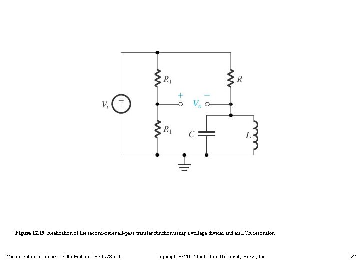
Figure 12. 19 Realization of the second-order all-pass transfer function using a voltage divider and an LCR resonator. Microelectronic Circuits - Fifth Edition Sedra/Smith Copyright 2004 by Oxford University Press, Inc. 22

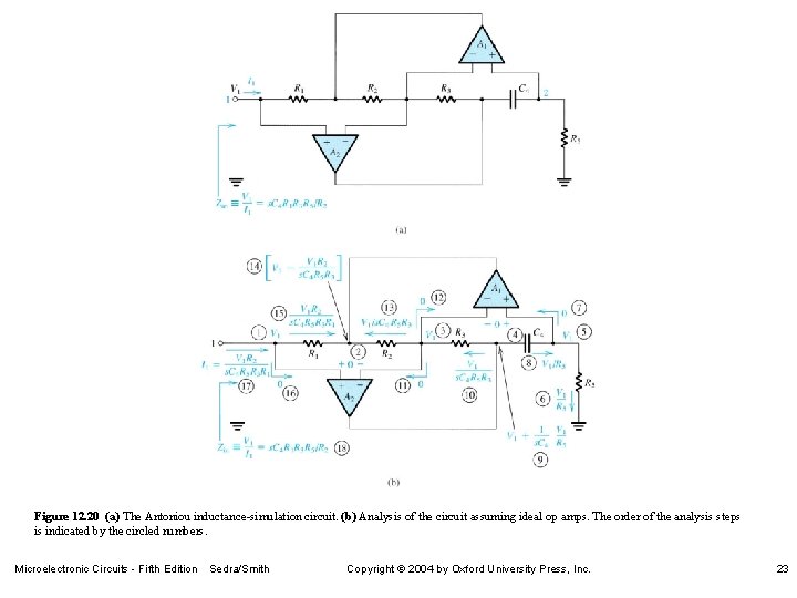
Figure 12. 20 (a) The Antoniou inductance-simulation circuit. (b) Analysis of the circuit assuming ideal op amps. The order of the analysis steps is indicated by the circled numbers. Microelectronic Circuits - Fifth Edition Sedra/Smith Copyright 2004 by Oxford University Press, Inc. 23

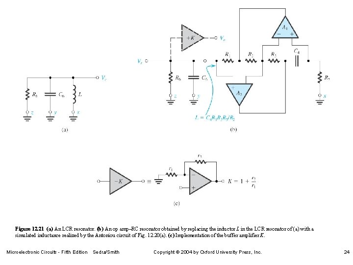
Figure 12. 21 (a) An LCR resonator. (b) An op amp–RC resonator obtained by replacing the inductor L in the LCR resonator of (a) with a simulated inductance realized by the Antoniou circuit of Fig. 12. 20(a). (c) Implementation of the buffer amplifier K. Microelectronic Circuits - Fifth Edition Sedra/Smith Copyright 2004 by Oxford University Press, Inc. 24

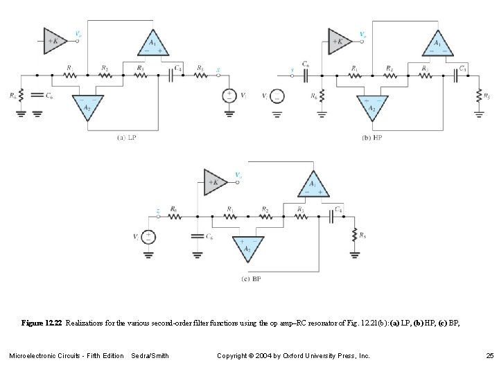
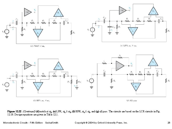
Figure 12. 22 Realizations for the various second-order filter functions using the op amp–RC resonator of Fig. 12. 21(b): (a) LP, (b) HP, (c) BP, Microelectronic Circuits - Fifth Edition Sedra/Smith Copyright 2004 by Oxford University Press, Inc. 25

Figure 12. 22 (Continued) (d) notch at w 0, (e) LPN, wn ³ w 0, (f) HPN, wn £ w 0, and (g) all pass. The circuits are based on the LCR circuits in Fig. 12. 18. Design equations are given in Table 12. 1. Microelectronic Circuits - Fifth Edition Sedra/Smith Copyright 2004 by Oxford University Press, Inc. 26

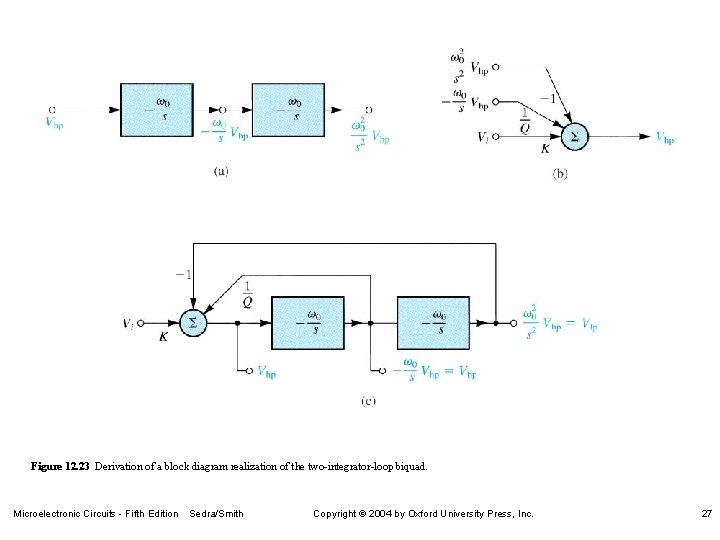
Figure 12. 23 Derivation of a block diagram realization of the two-integrator-loop biquad. Microelectronic Circuits - Fifth Edition Sedra/Smith Copyright 2004 by Oxford University Press, Inc. 27

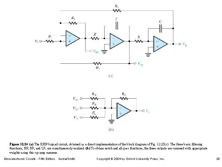
Figure 12. 24 (a) The KHN biquad circuit, obtained as a direct implementation of the block diagram of Fig. 12. 23(c). The three basic filtering functions, HP, BP, and LP, are simultaneously realized. (b) To obtain notch and all-pass functions, the three outputs are summed with appropriate weights using this op-amp summer. Microelectronic Circuits - Fifth Edition Sedra/Smith Copyright 2004 by Oxford University Press, Inc. 28

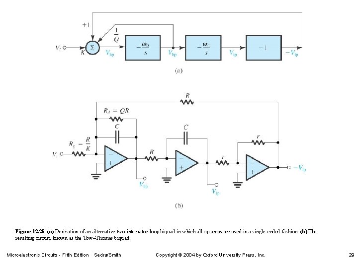
Figure 12. 25 (a) Derivation of an alternative two-integrator-loop biquad in which all op amps are used in a single-ended fashion. (b) The resulting circuit, known as the Tow–Thomas biquad. Microelectronic Circuits - Fifth Edition Sedra/Smith Copyright 2004 by Oxford University Press, Inc. 29

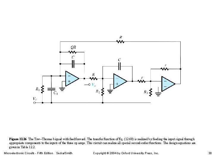
Figure 12. 26 The Tow–Thomas biquad with feedforward. The transfer function of Eq. (12. 68) is realized by feeding the input signal through appropriate components to the inputs of the three op amps. This circuit can realize all special second-order functions. The design equations are given in Table 12. 2. Microelectronic Circuits - Fifth Edition Sedra/Smith Copyright 2004 by Oxford University Press, Inc. 30

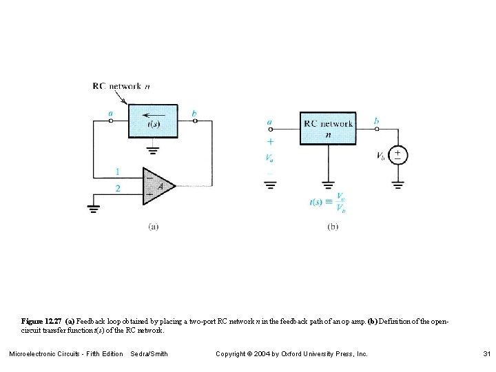
Figure 12. 27 (a) Feedback loop obtained by placing a two-port RC network n in the feedback path of an op amp. (b) Definition of the opencircuit transfer function t(s) of the RC network. Microelectronic Circuits - Fifth Edition Sedra/Smith Copyright 2004 by Oxford University Press, Inc. 31

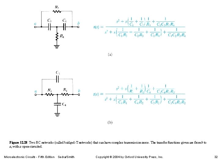
Figure 12. 28 Two RC networks (called bridged-T networks) that can have complex transmission zeros. The transfer functions given are from b to a, with a open-circuited. Microelectronic Circuits - Fifth Edition Sedra/Smith Copyright 2004 by Oxford University Press, Inc. 32

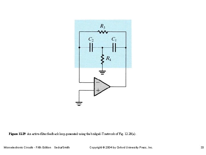
Figure 12. 29 An active-filter feedback loop generated using the bridged-T network of Fig. 12. 28(a). Microelectronic Circuits - Fifth Edition Sedra/Smith Copyright 2004 by Oxford University Press, Inc. 33

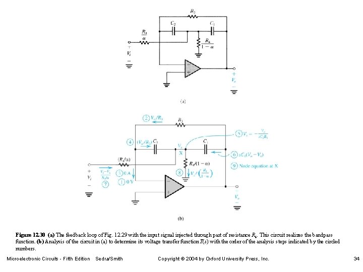
Figure 12. 30 (a) The feedback loop of Fig. 12. 29 with the input signal injected through part of resistance R 4. This circuit realizes the bandpass function. (b) Analysis of the circuit in (a) to determine its voltage transfer function T(s) with the order of the analysis steps indicated by the circled numbers. Microelectronic Circuits - Fifth Edition Sedra/Smith Copyright 2004 by Oxford University Press, Inc. 34

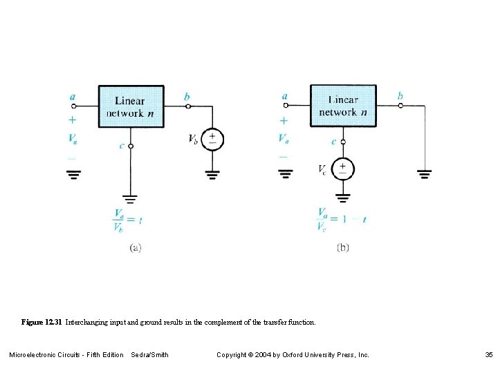
Figure 12. 31 Interchanging input and ground results in the complement of the transfer function. Microelectronic Circuits - Fifth Edition Sedra/Smith Copyright 2004 by Oxford University Press, Inc. 35

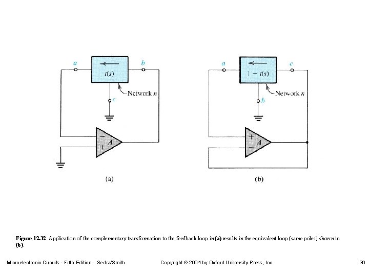
Figure 12. 32 Application of the complementary transformation to the feedback loop in (a) results in the equivalent loop (same poles) shown in (b). Microelectronic Circuits - Fifth Edition Sedra/Smith Copyright 2004 by Oxford University Press, Inc. 36

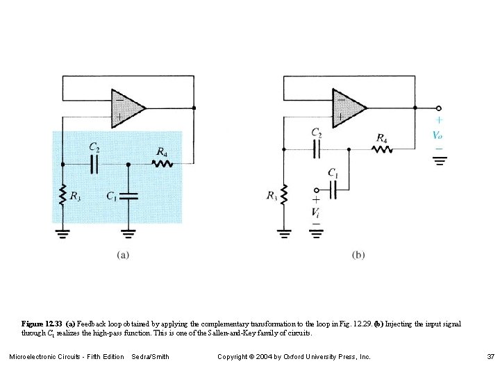
Figure 12. 33 (a) Feedback loop obtained by applying the complementary transformation to the loop in Fig. 12. 29. (b) Injecting the input signal through C 1 realizes the high-pass function. This is one of the Sallen-and-Key family of circuits. Microelectronic Circuits - Fifth Edition Sedra/Smith Copyright 2004 by Oxford University Press, Inc. 37

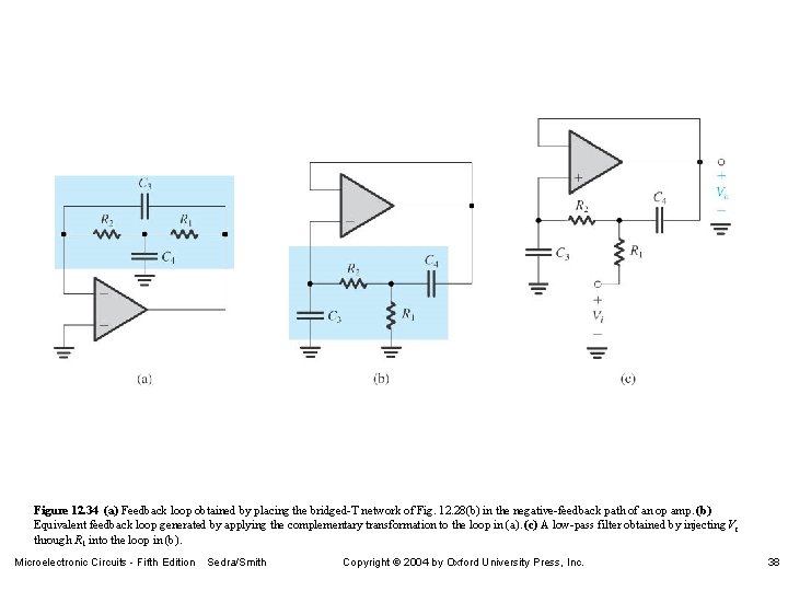
Figure 12. 34 (a) Feedback loop obtained by placing the bridged-T network of Fig. 12. 28(b) in the negative-feedback path of an op amp. (b) Equivalent feedback loop generated by applying the complementary transformation to the loop in (a). (c) A low-pass filter obtained by injecting Vi through R 1 into the loop in (b). Microelectronic Circuits - Fifth Edition Sedra/Smith Copyright 2004 by Oxford University Press, Inc. 38

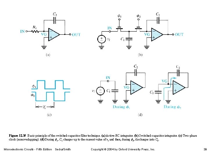
Figure 12. 35 Basic principle of the switched-capacitor filter technique. (a) Active-RC integrator. (b) Switched-capacitor integrator. (c) Two-phase clock (nonoverlapping). (d) During f 1, C 1 charges up to the current value of vi and then, during f 2, discharges into C 2. Microelectronic Circuits - Fifth Edition Sedra/Smith Copyright 2004 by Oxford University Press, Inc. 39

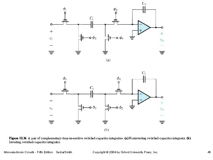
Figure 12. 36 A pair of complementary stray-insensitive switched-capacitor integrators. (a) Noninverting switched-capacitor integrator. (b) Inverting switched-capacitor integrator. Microelectronic Circuits - Fifth Edition Sedra/Smith Copyright 2004 by Oxford University Press, Inc. 40

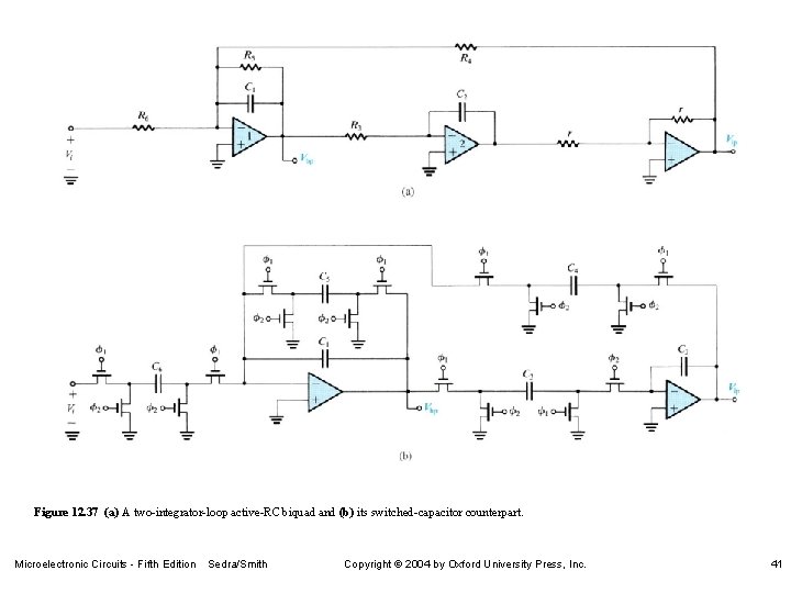
Figure 12. 37 (a) A two-integrator-loop active-RC biquad and (b) its switched-capacitor counterpart. Microelectronic Circuits - Fifth Edition Sedra/Smith Copyright 2004 by Oxford University Press, Inc. 41

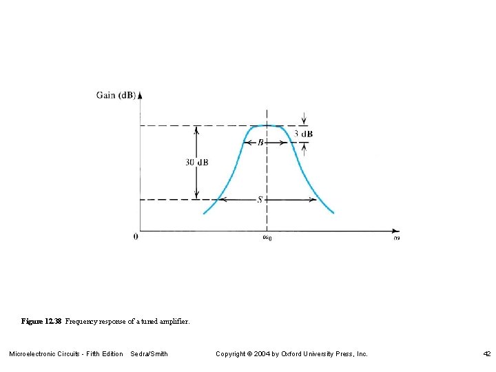
Figure 12. 38 Frequency response of a tuned amplifier. Microelectronic Circuits - Fifth Edition Sedra/Smith Copyright 2004 by Oxford University Press, Inc. 42

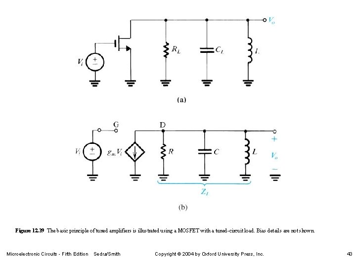
Figure 12. 39 The basic principle of tuned amplifiers is illustrated using a MOSFET with a tuned-circuit load. Bias details are not shown. Microelectronic Circuits - Fifth Edition Sedra/Smith Copyright 2004 by Oxford University Press, Inc. 43

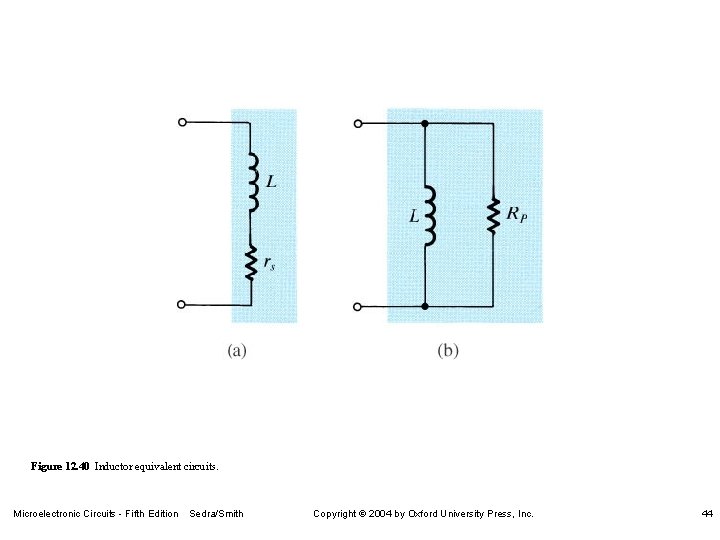
Figure 12. 40 Inductor equivalent circuits. Microelectronic Circuits - Fifth Edition Sedra/Smith Copyright 2004 by Oxford University Press, Inc. 44

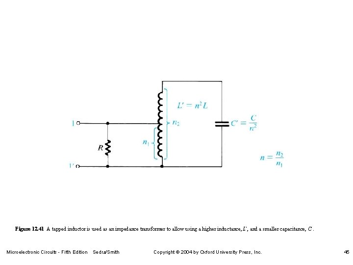
Figure 12. 41 A tapped inductor is used as an impedance transformer to allow using a higher inductance, L¢, and a smaller capacitance, C¢. Microelectronic Circuits - Fifth Edition Sedra/Smith Copyright 2004 by Oxford University Press, Inc. 45

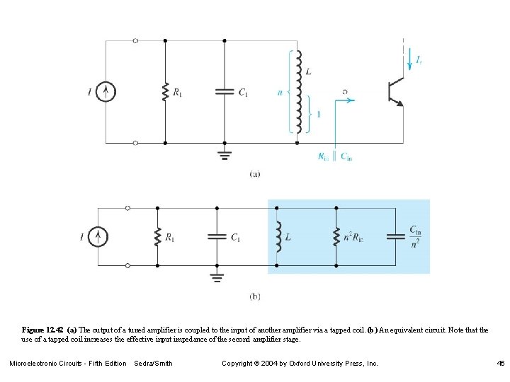
Figure 12. 42 (a) The output of a tuned amplifier is coupled to the input of another amplifier via a tapped coil. (b) An equivalent circuit. Note that the use of a tapped coil increases the effective input impedance of the second amplifier stage. Microelectronic Circuits - Fifth Edition Sedra/Smith Copyright 2004 by Oxford University Press, Inc. 46

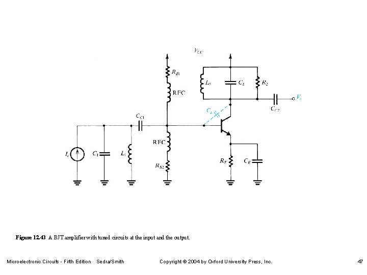
Figure 12. 43 A BJT amplifier with tuned circuits at the input and the output. Microelectronic Circuits - Fifth Edition Sedra/Smith Copyright 2004 by Oxford University Press, Inc. 47

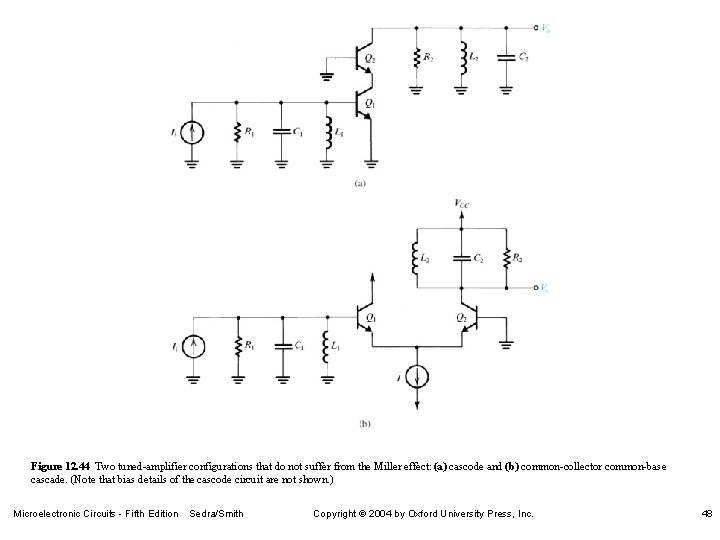
Figure 12. 44 Two tuned-amplifier configurations that do not suffer from the Miller effect: (a) cascode and (b) common-collector common-base cascade. (Note that bias details of the cascode circuit are not shown. ) Microelectronic Circuits - Fifth Edition Sedra/Smith Copyright 2004 by Oxford University Press, Inc. 48

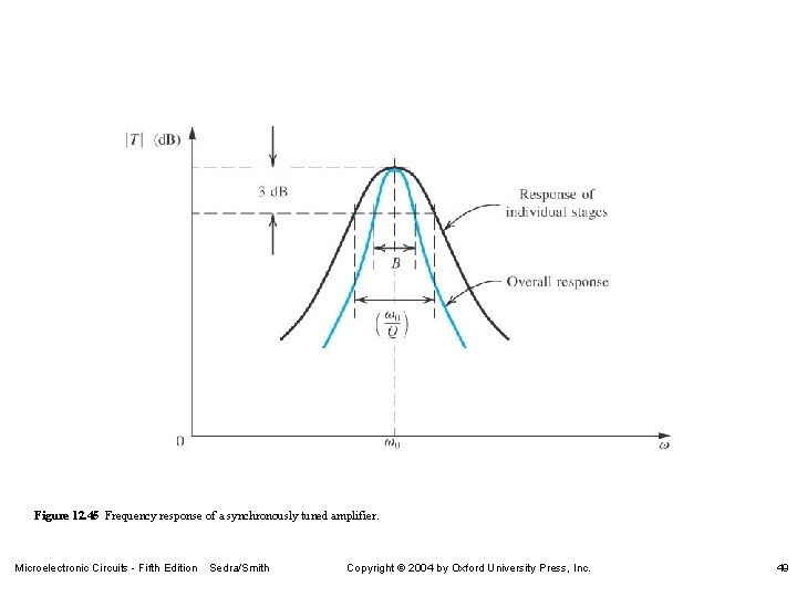
Figure 12. 45 Frequency response of a synchronously tuned amplifier. Microelectronic Circuits - Fifth Edition Sedra/Smith Copyright 2004 by Oxford University Press, Inc. 49

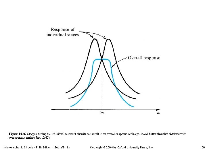
Figure 12. 46 Stagger-tuning the individual resonant circuits can result in an overall response with a passband flatter than that obtained with synchronous tuning (Fig. 12. 45). Microelectronic Circuits - Fifth Edition Sedra/Smith Copyright 2004 by Oxford University Press, Inc. 50

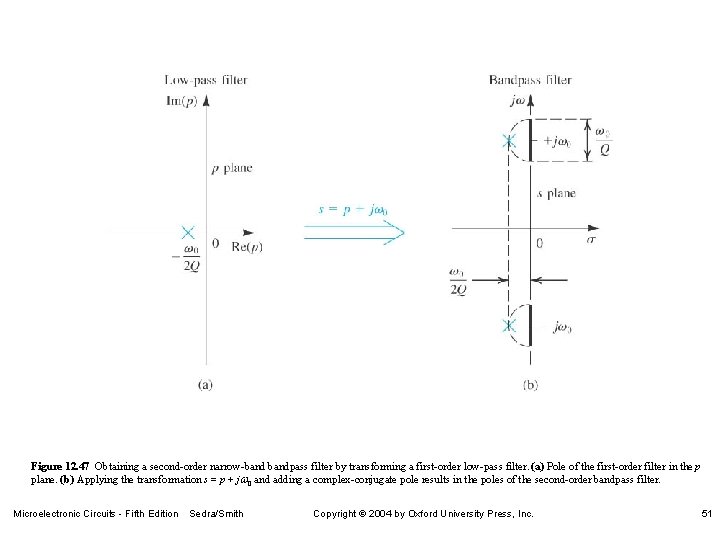
Figure 12. 47 Obtaining a second-order narrow-bandpass filter by transforming a first-order low-pass filter. (a) Pole of the first-order filter in the p plane. (b) Applying the transformation s = p + jw 0 and adding a complex-conjugate pole results in the poles of the second-order bandpass filter. Microelectronic Circuits - Fifth Edition Sedra/Smith Copyright 2004 by Oxford University Press, Inc. 51

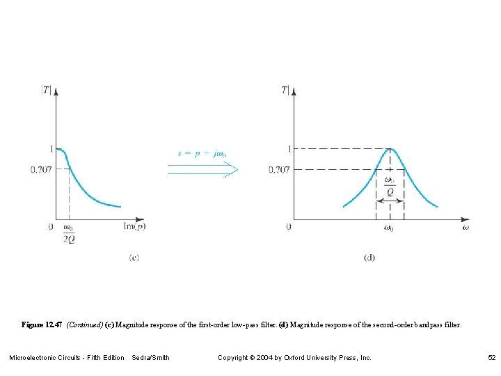
Figure 12. 47 (Continued) (c) Magnitude response of the first-order low-pass filter. (d) Magnitude response of the second-order bandpass filter. Microelectronic Circuits - Fifth Edition Sedra/Smith Copyright 2004 by Oxford University Press, Inc. 52

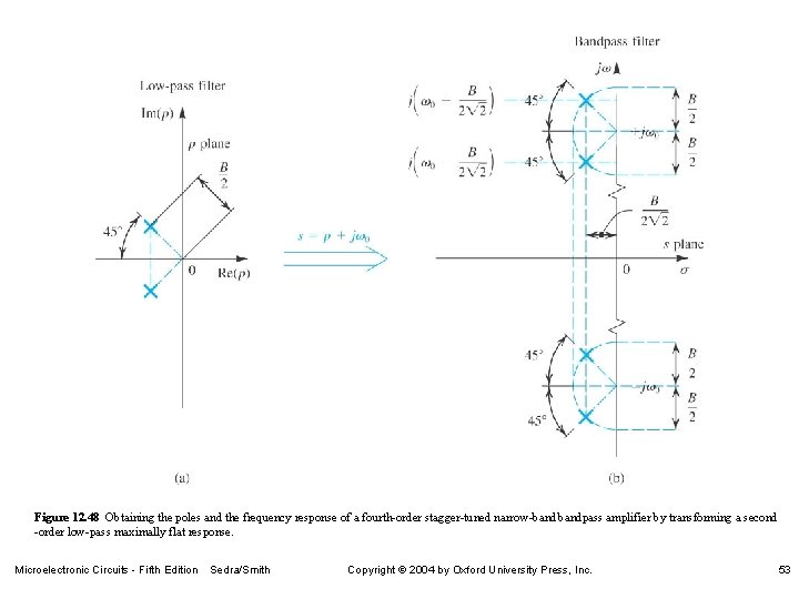
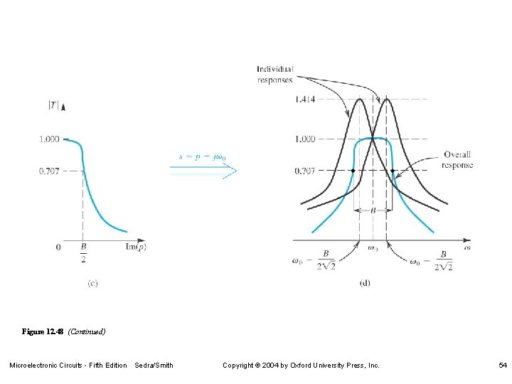
Figure 12. 48 Obtaining the poles and the frequency response of a fourth-order stagger-tuned narrow-bandpass amplifier by transforming a second -order low-pass maximally flat response. Microelectronic Circuits - Fifth Edition Sedra/Smith Copyright 2004 by Oxford University Press, Inc. 53

Figure 12. 48 (Continued) Microelectronic Circuits - Fifth Edition Sedra/Smith Copyright 2004 by Oxford University Press, Inc. 54

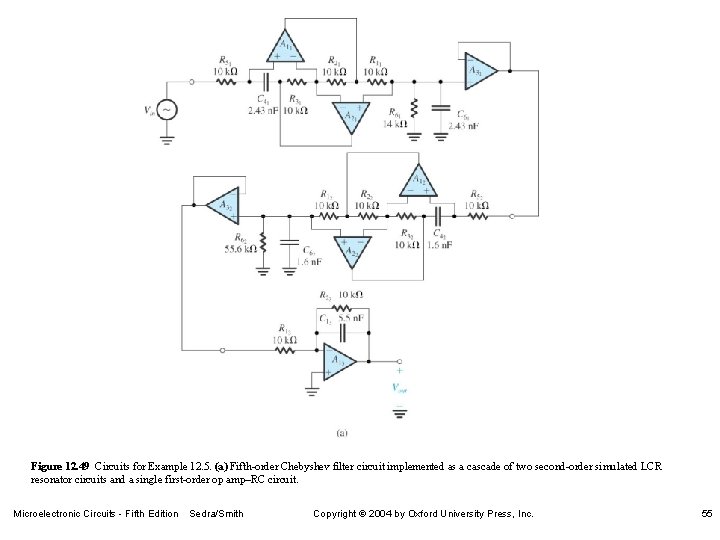
Figure 12. 49 Circuits for Example 12. 5. (a) Fifth-order Chebyshev filter circuit implemented as a cascade of two second-order simulated LCR resonator circuits and a single first-order op amp–RC circuit. Microelectronic Circuits - Fifth Edition Sedra/Smith Copyright 2004 by Oxford University Press, Inc. 55

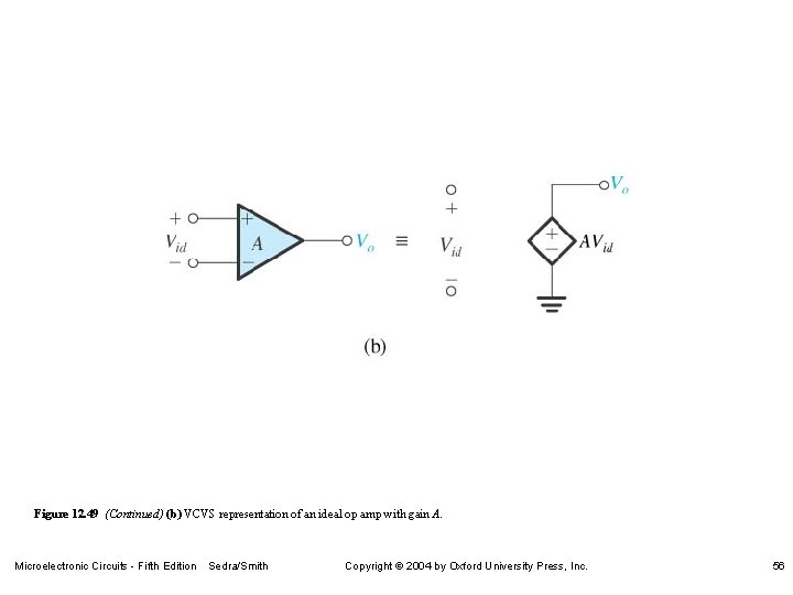
Figure 12. 49 (Continued) (b) VCVS representation of an ideal op amp with gain A. Microelectronic Circuits - Fifth Edition Sedra/Smith Copyright 2004 by Oxford University Press, Inc. 56

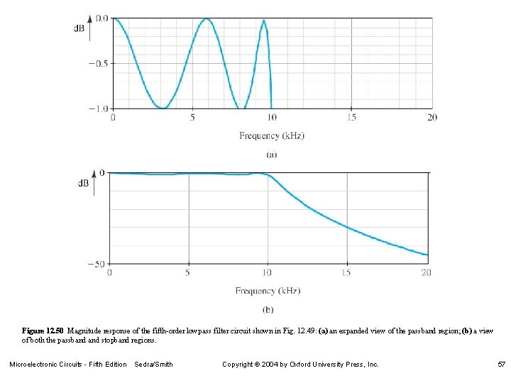
Figure 12. 50 Magnitude response of the fifth-order lowpass filter circuit shown in Fig. 12. 49: (a) an expanded view of the passband region; (b) a view of both the passband stopband regions. Microelectronic Circuits - Fifth Edition Sedra/Smith Copyright 2004 by Oxford University Press, Inc. 57

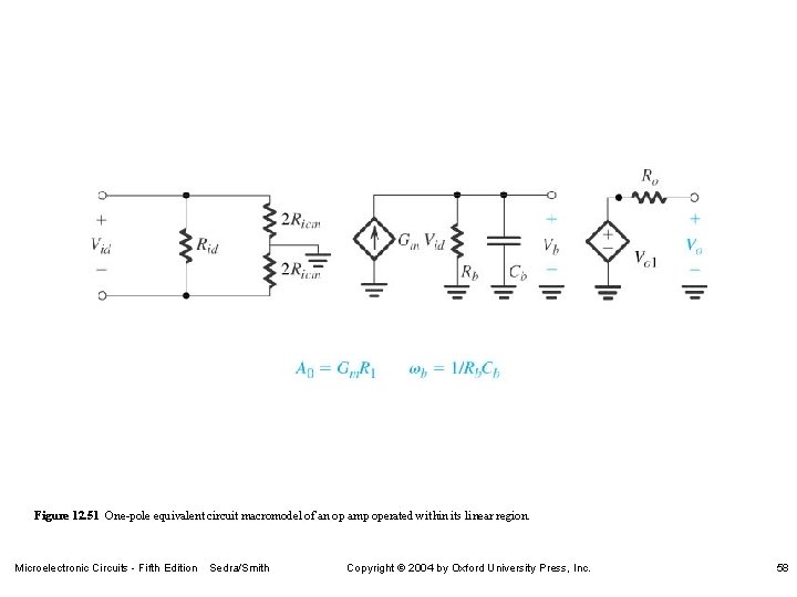
Figure 12. 51 One-pole equivalent circuit macromodel of an op amp operated within its linear region. Microelectronic Circuits - Fifth Edition Sedra/Smith Copyright 2004 by Oxford University Press, Inc. 58

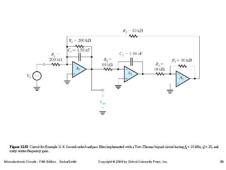
Figure 12. 52 Circuit for Example 11. 6. Second-order bandpass filter implemented with a Tow–Thomas biquad circuit having f 0 = 10 k. Hz, Q = 20, and unity center-frequency gain. Microelectronic Circuits - Fifth Edition Sedra/Smith Copyright 2004 by Oxford University Press, Inc. 59

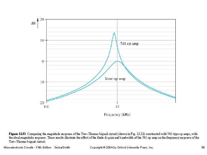
Figure 12. 53 Comparing the magnitude response of the Tow–Thomas biquad circuit (shown in Fig. 12. 52) constructed with 741 -type op amps, with the ideal magnitude response. These results illustrate the effect of the finite dc gain and bandwidth of the 741 op amp on the frequency response of the Tow–Thomas biquad circuit. Microelectronic Circuits - Fifth Edition Sedra/Smith Copyright 2004 by Oxford University Press, Inc. 60

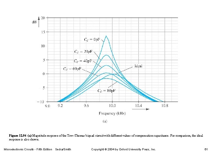
Figure 12. 54 (a) Magnitude response of the Tow–Thomas biquad circuit with different values of compensation capacitance. For comparison, the ideal response is also shown. Microelectronic Circuits - Fifth Edition Sedra/Smith Copyright 2004 by Oxford University Press, Inc. 61

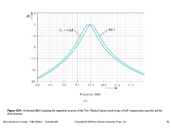
Figure 12. 54 (Continued) (b) Comparing the magnitude response of the Tow–Thomas biquad circuit using a 64 -p. F compensation capacitor and the ideal response. Microelectronic Circuits - Fifth Edition Sedra/Smith Copyright 2004 by Oxford University Press, Inc. 62

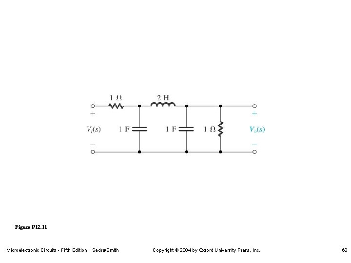
Figure P 12. 11 Microelectronic Circuits - Fifth Edition Sedra/Smith Copyright 2004 by Oxford University Press, Inc. 63

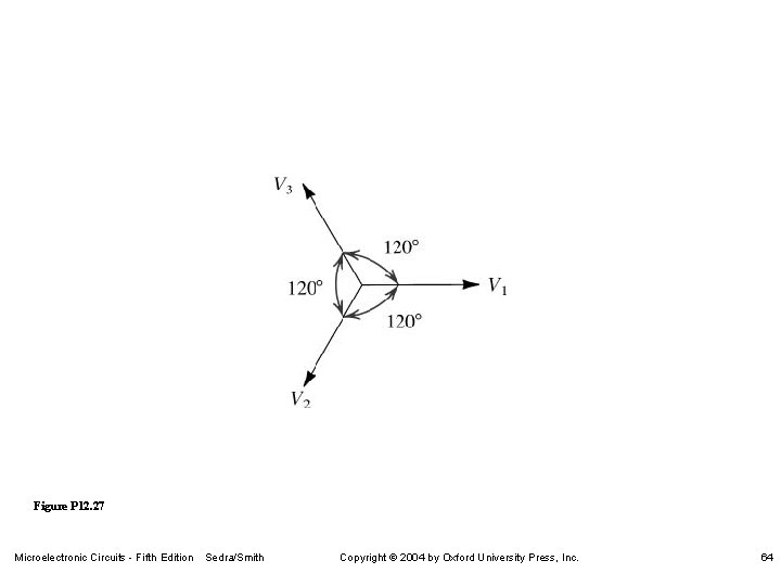
Figure P 12. 27 Microelectronic Circuits - Fifth Edition Sedra/Smith Copyright 2004 by Oxford University Press, Inc. 64