Resistive Strips foils production for ATLAS NSW Micro
- Slides: 25

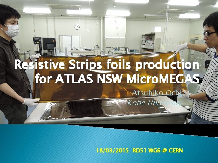
Resistive Strips foils production for ATLAS NSW Micro. MEGAS Atsuhiko Ochi, Kobe University 18/03/2015 RD 51 WG 6 @ CERN

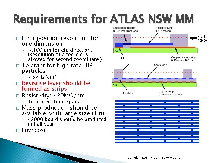
Requirements for ATLAS NSW MM � High position resolution for one dimension ◦ � <100 μm for eta direction. (Resolution of a few cm is allowed for second coordinate. ) Mesh (GND) +HV Tolerant for high rate HIP particles ◦ ~ 5 k. Hz/cm 2 � � Resistive layer should be formed as strips Resistivity: ~20 MΩ/cm ◦ To protect from spark � Mass production should be available, with large size (1 m) ◦ ~2000 board should be produced in half year. � Low cost A. Ochi, RD 51 WG 6 18/03/2015

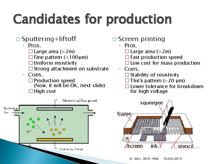
Candidates for production � Sputtering+liftoff ◦ Pros. � Large area (>2 m) � Fine pattern (<100μm) � Uniform resistivity � Strong attachment on substrate ◦ Cons. � Production speed (Now, it will be OK, next slide) � High cost � Screen printing ◦ Pros. � Large area (>2 m) � Fast production speed � Low cost for mass production ◦ Cons. � Stability of resistivity � Thick pattern (~20 μm) � Lower tolerance for breakdown for high voltage squeegee frame Screen ink A. Ochi, RD 51 WG 6 stencil 18/03/2015

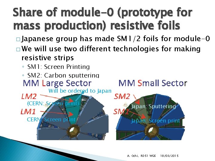
Share of module-0 (prototype for mass production) resistive foils � Japanese group has made SM 1/2 foils for module-0 � We will use two different technologies for making resistive strips ◦ SM 1: Screen Printing ◦ SM 2: Carbon sputtering Will be ordered to Japan (CERN: Screen print) CERN: Screen print Japan: Sputtering Japan: Screen print A. Ochi, RD 51 WG 6 18/03/2015

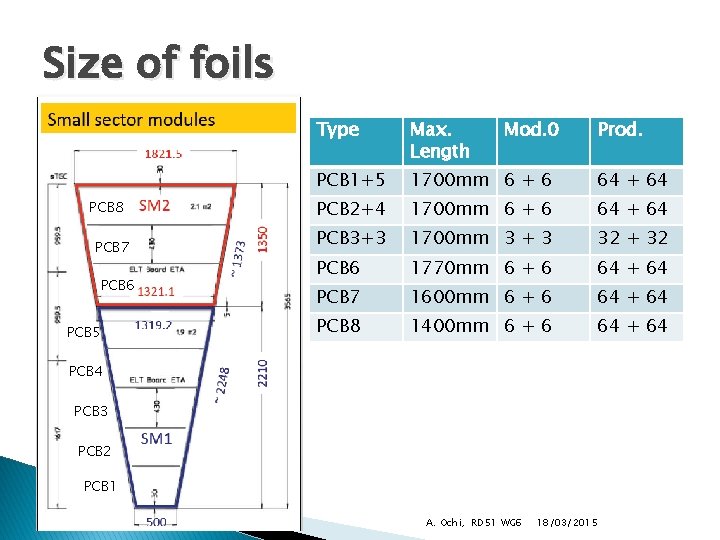
Size of foils PCB 8 PCB 7 PCB 6 PCB 5 Type Max. Length Mod. 0 Prod. PCB 1+5 1700 mm 6 + 6 64 + 64 PCB 2+4 1700 mm 6 + 6 64 + 64 PCB 3+3 1700 mm 3 + 3 32 + 32 PCB 6 1770 mm 6 + 6 64 + 64 PCB 7 1600 mm 6 + 6 64 + 64 PCB 8 1400 mm 6 + 6 64 + 64 PCB 3 PCB 2 PCB 1 A. Ochi, RD 51 WG 6 18/03/2015

Screen printing A. Ochi, RD 51 WG 6 18/03/2015

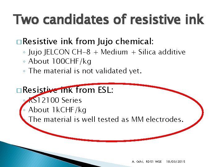
Two candidates of resistive ink � Resistive ink from Jujo chemical: � Resistive ink from ESL: ◦ Jujo JELCON CH-8 + Medium + Silica additive ◦ About 100 CHF/kg ◦ The material is not validated yet. ◦ RS 12100 Series ◦ About 1 k. CHF/kg ◦ The material is well tested as MM electrodes. A. Ochi, RD 51 WG 6 18/03/2015

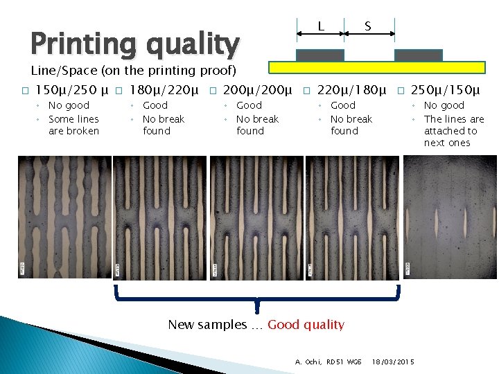
L Printing quality S Line/Space (on the printing proof) � 150μ/250 μ ◦ No good ◦ Some lines are broken � 180μ/220μ ◦ Good ◦ No break found � 200μ/200μ ◦ Good ◦ No break found � 220μ/180μ ◦ Good ◦ No break found � 250μ/150μ ◦ No good ◦ The lines are attached to next ones New samples … Good quality A. Ochi, RD 51 WG 6 18/03/2015

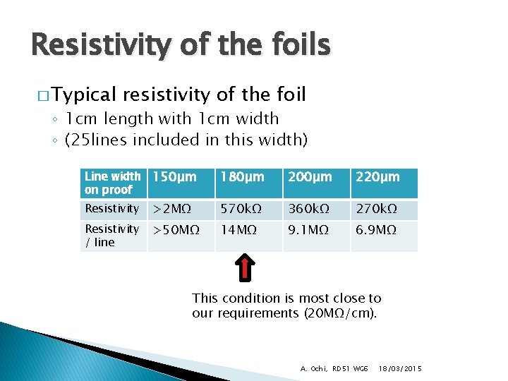
Resistivity of the foils � Typical resistivity of the foil ◦ 1 cm length with 1 cm width ◦ (25 lines included in this width) Line width on proof 150μm 180μm 200μm 220μm Resistivity >2 MΩ 570 kΩ 360 kΩ 270 kΩ Resistivity / line >50 MΩ 14 MΩ 9. 1 MΩ 6. 9 MΩ This condition is most close to our requirements (20 MΩ/cm). A. Ochi, RD 51 WG 6 18/03/2015

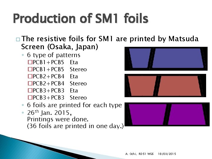
Production of SM 1 foils � The resistive foils for SM 1 are printed by Matsuda Screen (Osaka, Japan) ◦ 6 type of patterns �PCB 1+PCB 5 �PCB 2+PCB 4 �PCB 3+PCB 3 Eta Stereo ◦ 6 foils are printed for each type ◦ 26 th Jan. 2015, Printings were done. (36 foils are printed in one day. ) A. Ochi, RD 51 WG 6 18/03/2015

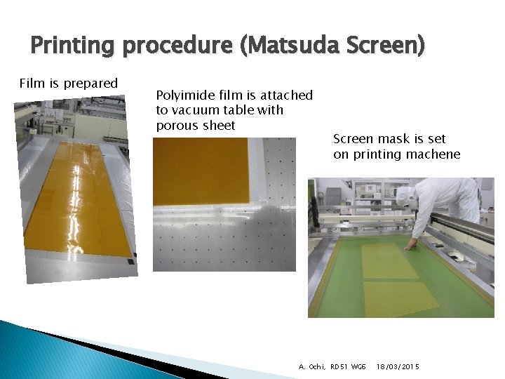
Printing procedure (Matsuda Screen) Film is prepared Polyimide film is attached to vacuum table with porous sheet Screen mask is set on printing machene A. Ochi, RD 51 WG 6 18/03/2015

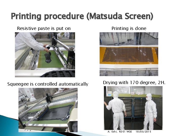
Printing procedure (Matsuda Screen) Resistive paste is put on Squeegee is controlled automatically Printing is done Drying with 170 degree, 2 H. A. Ochi, RD 51 WG 6 18/03/2015

Mass production feasibility � Screen print @ Matsuda Screen Inc. � Maximum size for printing ◦ 2600 mm x 1300 mm �We need 2200 mm x 500 mm maximum. � Production rate ◦ 50 foils / day �It is limited by ovens. � Production ◦ Reasonable cost A. Ochi, RD 51 WG 6 18/03/2015

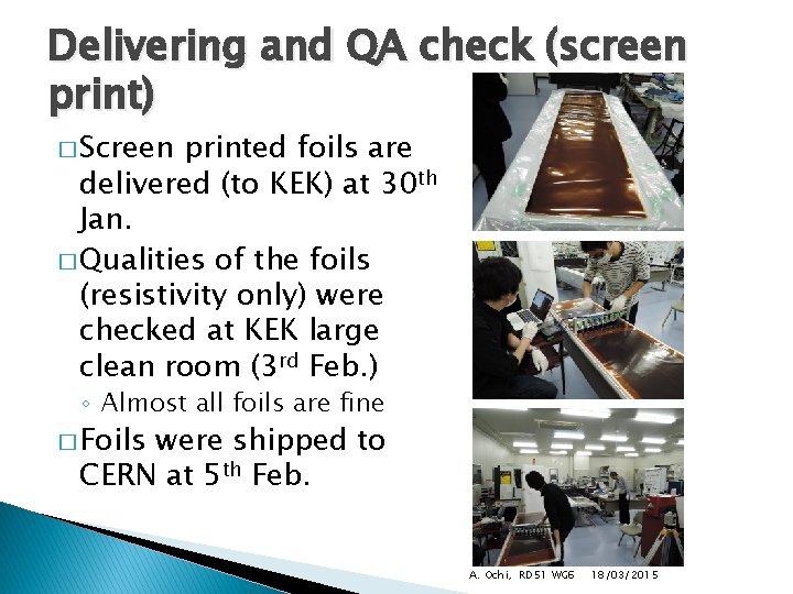
Delivering and QA check (screen print) � Screen printed foils are delivered (to KEK) at 30 th Jan. � Qualities of the foils (resistivity only) were checked at KEK large clean room (3 rd Feb. ) ◦ Almost all foils are fine � Foils were shipped to CERN at 5 th Feb. A. Ochi, RD 51 WG 6 18/03/2015

Carbon Sputtering A. Ochi, RD 51 WG 6 18/03/2015

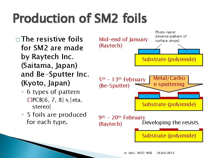
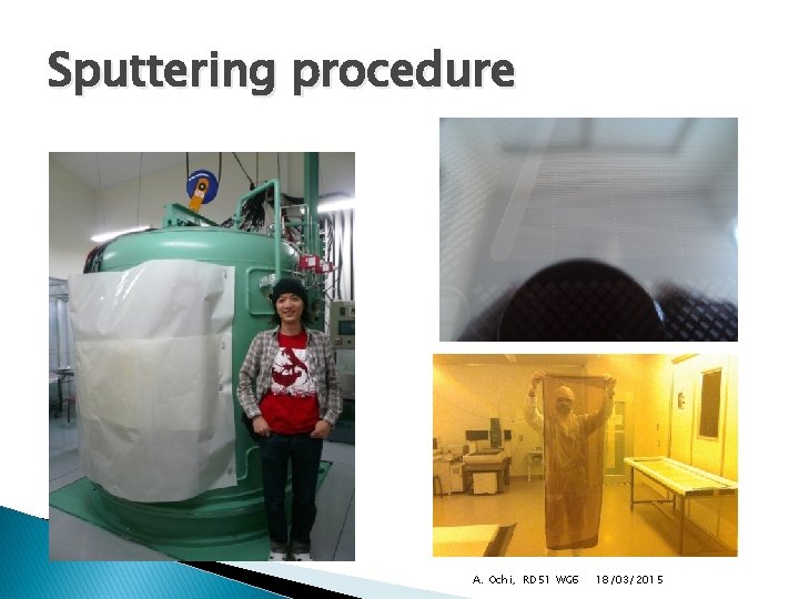
Production of SM 2 foils � The resistive foils for SM 2 are made by Raytech Inc. (Saitama, Japan) and Be-Sputter Inc. (Kyoto, Japan) ◦ 6 types of pattern �PCB{6, 7, 8} x {eta, stereo} ◦ 5 foils are produced for each type. Mid-end of January (Raytech) Photo resist (reverse pattern of surface strips) Substrate (polyimide) 5 th – 13 th February (Be-Sputter) Metal/Carbo n sputtering Substrate (polyimide) 9 th – 20 th February Developing the resists (Raytech) Substrate (polyimide) A. Ochi, RD 51 WG 6 18/03/2015

Sputtering procedure A. Ochi, RD 51 WG 6 18/03/2015

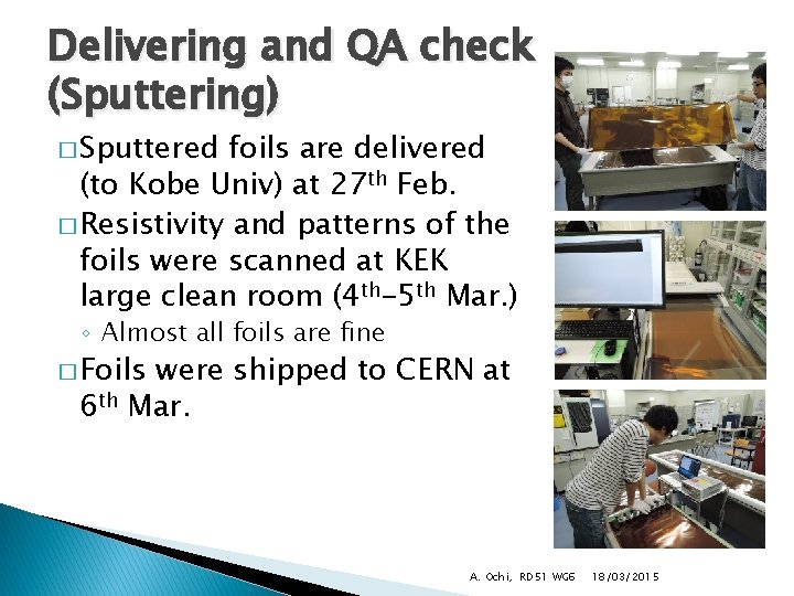
Delivering and QA check (Sputtering) � Sputtered foils are delivered (to Kobe Univ) at 27 th Feb. � Resistivity and patterns of the foils were scanned at KEK large clean room (4 th-5 th Mar. ) ◦ Almost all foils are fine � Foils were shipped to CERN at 6 th Mar. A. Ochi, RD 51 WG 6 18/03/2015

QA/QC A. Ochi, RD 51 WG 6 18/03/2015

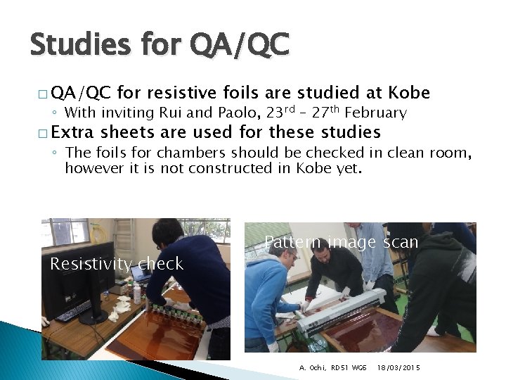
Studies for QA/QC � QA/QC for resistive foils are studied at Kobe ◦ With inviting Rui and Paolo, 23 rd – 27 th February � Extra sheets are used for these studies ◦ The foils for chambers should be checked in clean room, however it is not constructed in Kobe yet. Resistivity check Pattern image scan A. Ochi, RD 51 WG 6 18/03/2015

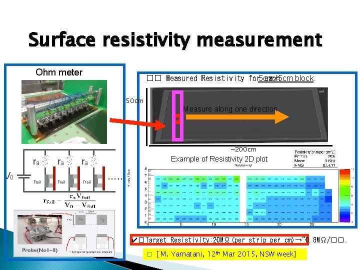
Surface resistivity measurement Ohm meter �� Measured Resistivity for 5 cm× 5 cm each block. 50 cm Measure along one direction ~200 cm V 0 ra ra ra rfoil Example of Resistivity 2 D plot ………. . ✔�Target Resistivity: 20 MΩ(per strip per cm)→~0. 8 MΩ/��. � [ M. Yamatani, 12 th Mar 2015, NSW week]

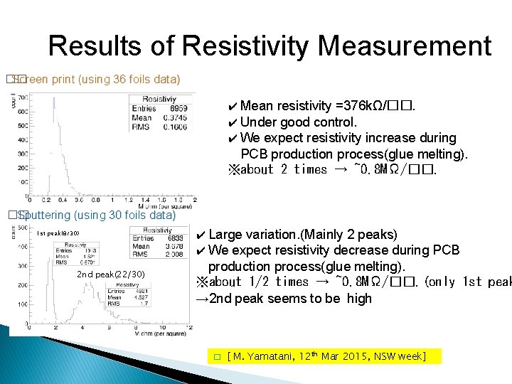
Results of Resistivity Measurement �� Screen print (using 36 foils data) ✔ Mean resistivity =376 kΩ/��. ✔ Under good control. ✔ We expect resistivity increase during PCB production process(glue melting). ※about 2 times → ~0. 8 MΩ/��. �� Sputtering (using 30 foils data) 1 st peak(8/30) 2 nd peak(22/30) ✔ Large variation. (Mainly 2 peaks) ✔ We expect resistivity decrease during PCB production process(glue melting). ※about 1/2 times → ~0. 8 MΩ/��. (only 1 st peak → 2 nd peak seems to be high � [ M. Yamatani, 12 th Mar 2015, NSW week]

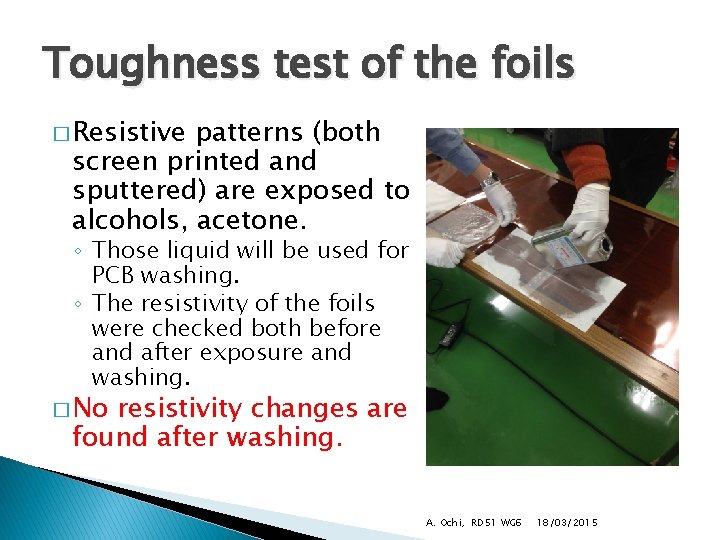
Toughness test of the foils � Resistive patterns (both screen printed and sputtered) are exposed to alcohols, acetone. ◦ Those liquid will be used for PCB washing. ◦ The resistivity of the foils were checked both before and after exposure and washing. � No resistivity changes are found after washing. A. Ochi, RD 51 WG 6 18/03/2015

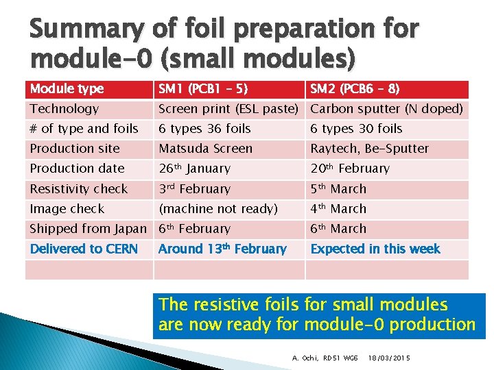
Summary of foil preparation for module-0 (small modules) Module type SM 1 (PCB 1 – 5) SM 2 (PCB 6 – 8) Technology Screen print (ESL paste) Carbon sputter (N doped) # of type and foils 6 types 36 foils 6 types 30 foils Production site Matsuda Screen Raytech, Be-Sputter Production date 26 th January 20 th February Resistivity check 3 rd February 5 th March Image check (machine not ready) 4 th March Shipped from Japan 6 th February 6 th March Delivered to CERN Expected in this week Around 13 th February The resistive foils for small modules are now ready for module-0 production A. Ochi, RD 51 WG 6 18/03/2015

Conclusion � Large area resistive strip foils (1800 x 500) have been produced for ATLAS NSW MM module-0. � Two different technologies are used for those production. ◦ Screen Print ◦ Carbon Sputtering � Both of them are successfully produced. ◦ We can keep two option for resistive foil production. ◦ The cost for screen print is much lower. A. Ochi, RD 51 WG 6 18/03/2015