Radiation Damage in Silicon Katharina Kaska TA 1


- Slides: 19
Radiation Damage in Silicon Katharina Kaska TA 1 -SD Alison Bates, Christian Joram, Michael Moll
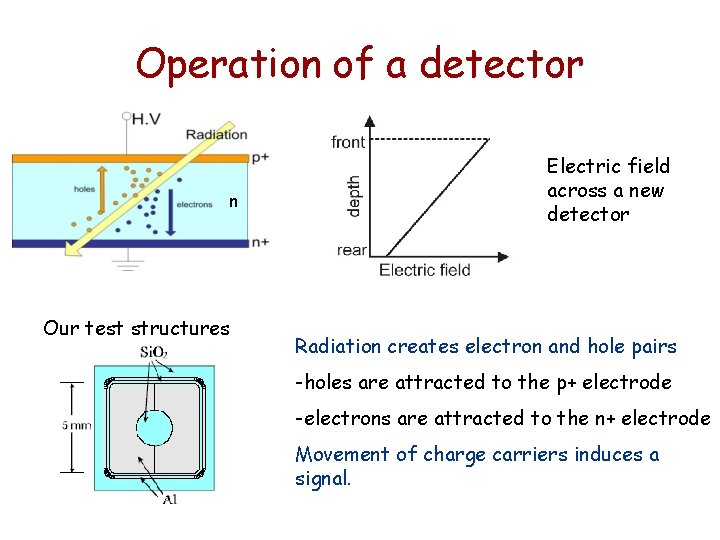
Operation of a detector n Our test structures Electric field across a new detector Radiation creates electron and hole pairs -holes are attracted to the p+ electrode -electrons are attracted to the n+ electrode Movement of charge carriers induces a signal.
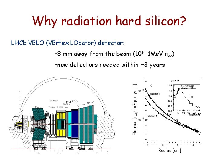
Why radiation hard silicon? LHCb VELO (VErtex LOcator) detector: • 8 mm away from the beam (1014 1 Me. V neq) Fluence [neq/cm 2 per year] • new detectors needed within ~3 years Radius [cm]
Defects in Silicon Main (macroscopic) effects of radiation damage in silicon: • Increased leakage current • Increased depletion voltage • Increased trapping
Types of Silicon Float Zone (FZ) silicon: 1 x 10 -15 cm-3 O 2 Oxygenated silicon: 1 x 10 -17 cm-3 O 2 Czochralski (CZ) silicon: 1 x 10 -18 cm-3 O 2 Oxygenated silicon seems to be better than Float Zone silicon.
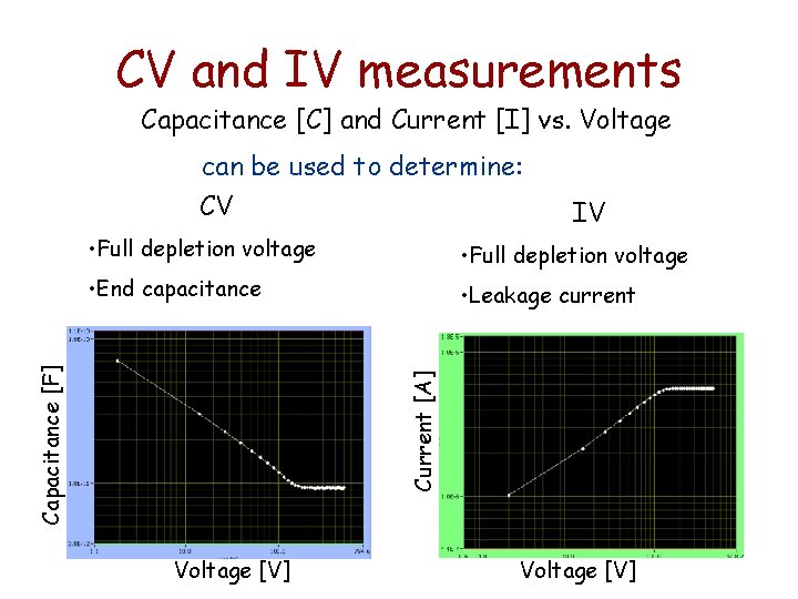
CV and IV measurements Capacitance [C] and Current [I] vs. Voltage can be used to determine: CV IV • Full depletion voltage • End capacitance • Leakage current Current [A] Capacitance [F] • Full depletion voltage Voltage [V]
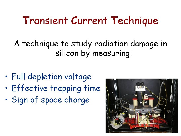
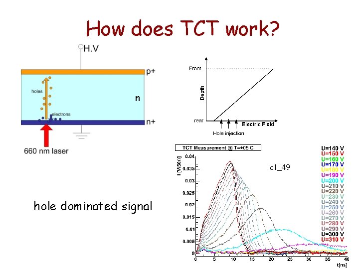
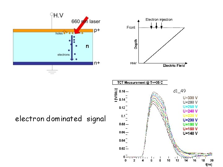
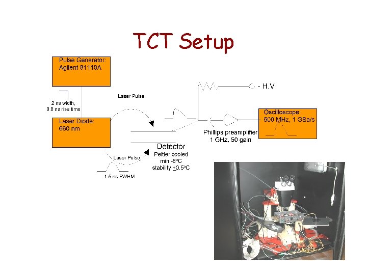
Transient Current Technique A technique to study radiation damage in silicon by measuring: • Full depletion voltage • Effective trapping time • Sign of space charge
How does TCT work? n d 1_49 hole dominated signal
n d 1_49 electron dominated signal
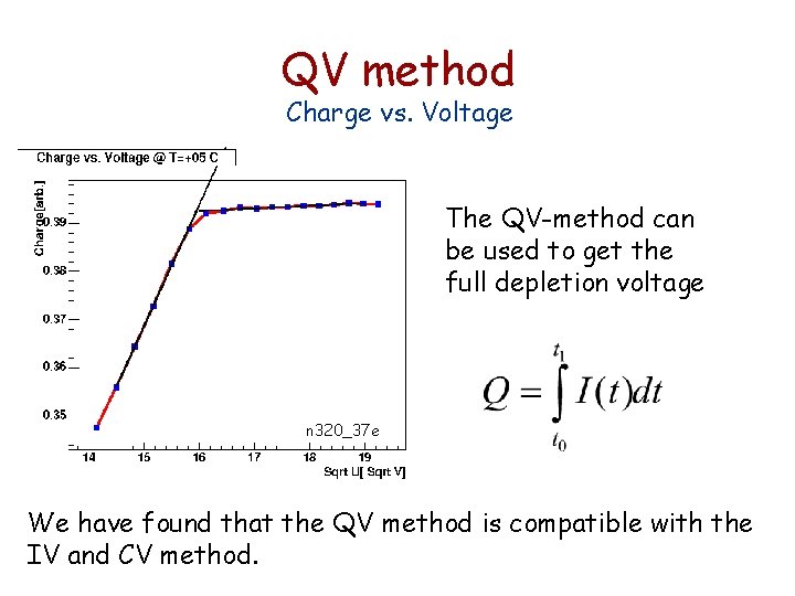
QV method Charge vs. Voltage The QV-method can be used to get the full depletion voltage n 320_37 e We have found that the QV method is compatible with the IV and CV method.
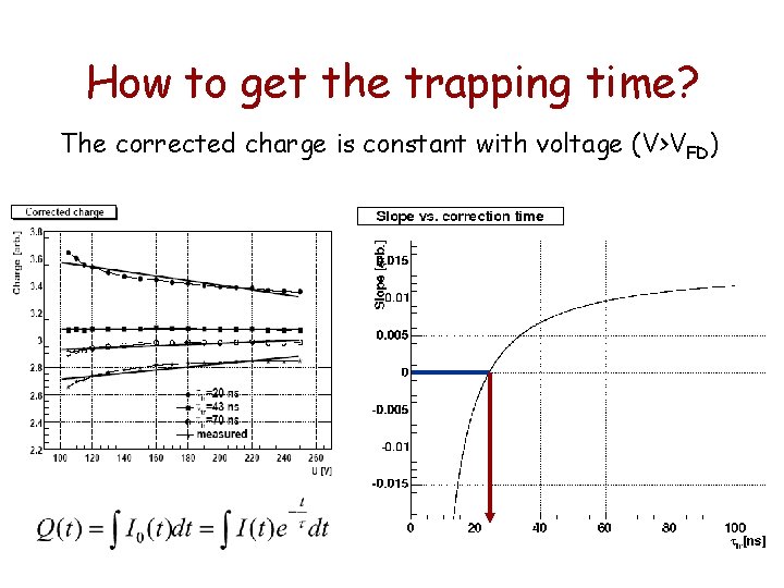
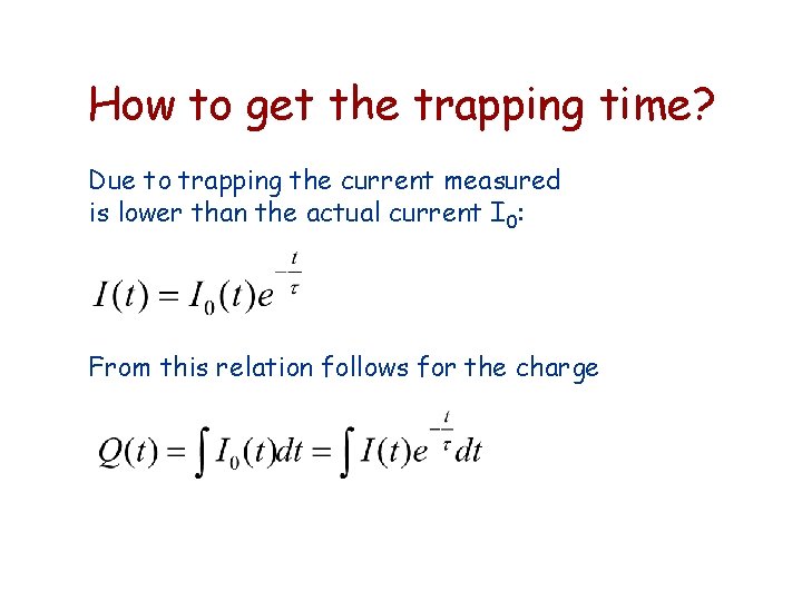
Effective trapping time Charge gets trapped in the detector due to radiation damage. The amount of charge trapped depends on the number of defects (hence on the fluence) and also on the applied voltage (over full depletion): Higher voltage -> higher drift velocity -> fewer charge carriers trapped -> more charge measured
How to get the trapping time? The corrected charge is constant with voltage (V>VFD)
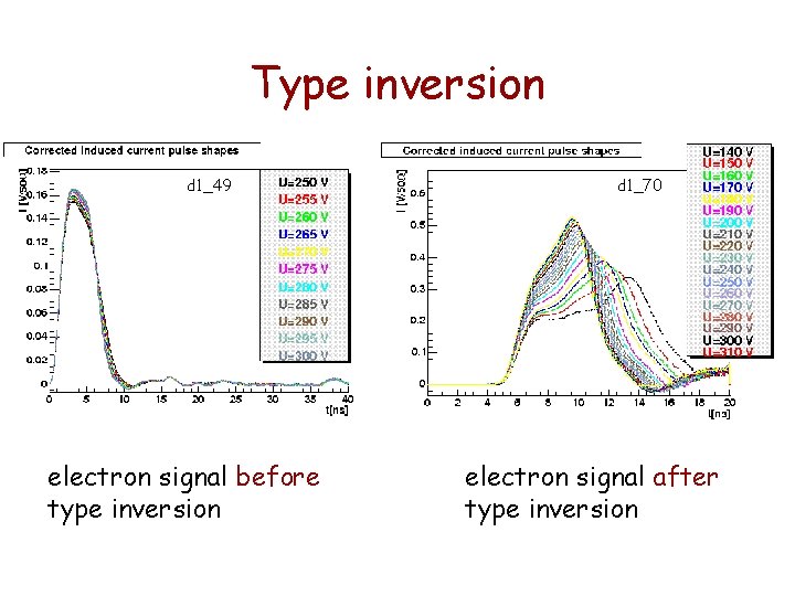
Type inversion d 1_49 d 1_70 f 2_69 h electron signal before type inversion electron signal after type inversion
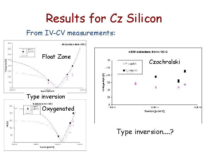
Results for Cz Silicon From IV-CV measurements: Float Zone Czochralski Type inversion Oxygenated Type inversion. . ?
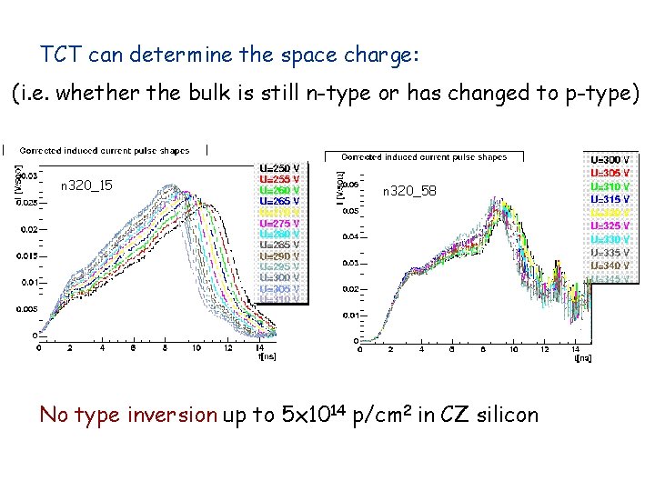
TCT can determine the space charge: (i. e. whether the bulk is still n-type or has changed to p-type) n 320_15 n 320_58 No type inversion up to 5 x 10¹⁴ p/cm 2 in CZ silicon
Conclusions • Float Zone and Oxygenated silicon type invert • The QV method is compatible to CV and IV • Czochralski silicon doesn‘t type invert QUESTIONS? ? ?
Irradiation and annealing The samples are irradiated with a fluence between 1012 – 1015 p/cm-2 (24 Ge. V protons) at IRRAD 1 (PS). Before measurements the detectors are annealed to remove movable carriers and get them all on the same damage level.
TCT Setup
How to get the trapping time? Due to trapping the current measured is lower than the actual current I 0: From this relation follows for the charge