Progress on Large Area GEMs 12 th Vienna

- Slides: 23

Progress on Large Area GEMs 12 th Vienna Conference on Instrumentation – VCI 2010 15 – 20 February 2010, Vienna Marco Villa, Matteo Alfonsi, Ian Brock, Gabriele Croci, Eric David, Rui de Oliveira, Serge Duarte Pinto, Elena Rocco, Leszek Ropelewski, Hans Taureg, Miranda van Stenis

Outline • Gas Electron Multipliers • GEM applications • Motivation for large area GEMs • Single mask photolithography • Improving the polyimide etching • Improving the bottom copper etching • Splicing GEMs • Stretching large area GEMs • Handling large area GEMs • Simulating GEMs • Optimizing the hole geometry • Understanding the charging up • Conclusions & outlooks

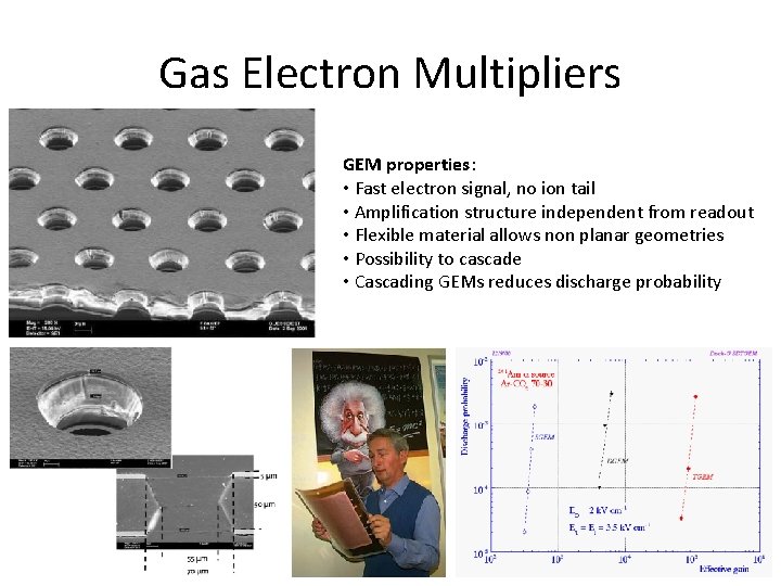
Gas Electron Multipliers GEM properties: • Fast electron signal, no ion tail • Amplification structure independent from readout • Flexible material allows non planar geometries • Possibility to cascade • Cascading GEMs reduces discharge probability

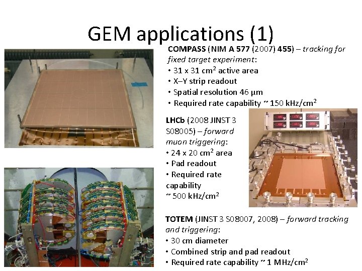
GEM applications (1) COMPASS (NIM A 577 (2007) 455) – tracking for fixed target experiment: • 31 x 31 cm 2 active area • X–Y strip readout • Spatial resolution 46 µm • Required rate capability ~ 150 k. Hz/cm 2 LHCb (2008 JINST 3 S 08005) – forward muon triggering: • 24 x 20 cm 2 area • Pad readout • Required rate capability ~ 500 k. Hz/cm 2 TOTEM (JINST 3 S 08007, 2008) – forward tracking and triggering: • 30 cm diameter • Combined strip and pad readout • Required rate capability ~ 1 MHz/cm 2

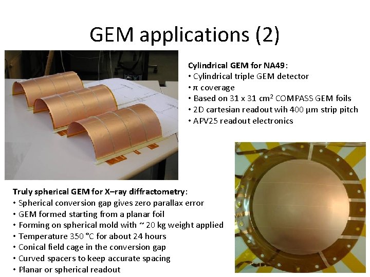
GEM applications (2) Cylindrical GEM for NA 49: • Cylindrical triple GEM detector • π coverage • Based on 31 x 31 cm 2 COMPASS GEM foils • 2 D cartesian readout wih 400 µm strip pitch • APV 25 readout electronics Truly spherical GEM for X–ray diffractometry: • Spherical conversion gap gives zero parallax error • GEM formed starting from a planar foil • Forming on spherical mold with ~ 20 kg weight applied • Temperature 350 °C for about 24 hours • Conical field cage in the conversion gap • Curved spacers to keep accurate spacing • Planar or spherical readout

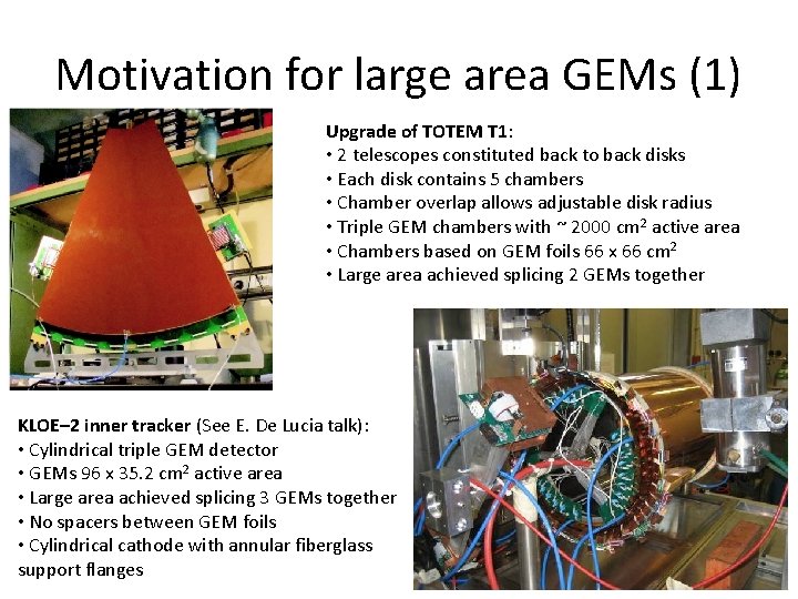
Motivation for large area GEMs (1) Upgrade of TOTEM T 1: • 2 telescopes constituted back to back disks • Each disk contains 5 chambers • Chamber overlap allows adjustable disk radius • Triple GEM chambers with ~ 2000 cm 2 active area • Chambers based on GEM foils 66 x 66 cm 2 • Large area achieved splicing 2 GEMs together KLOE– 2 inner tracker (See E. De Lucia talk): • Cylindrical triple GEM detector • GEMs 96 x 35. 2 cm 2 active area • Large area achieved splicing 3 GEMs together • No spacers between GEM foils • Cylindrical cathode with annular fiberglass support flanges

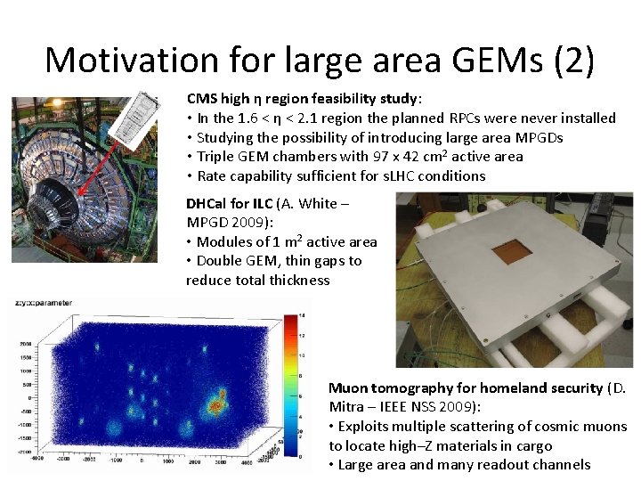
Motivation for large area GEMs (2) CMS high η region feasibility study: • In the 1. 6 < η < 2. 1 region the planned RPCs were never installed • Studying the possibility of introducing large area MPGDs • Triple GEM chambers with 97 x 42 cm 2 active area • Rate capability sufficient for s. LHC conditions DHCal for ILC (A. White – MPGD 2009): • Modules of 1 m 2 active area • Double GEM, thin gaps to reduce total thickness Muon tomography for homeland security (D. Mitra – IEEE NSS 2009): • Exploits multiple scattering of cosmic muons to locate high–Z materials in cargo • Large area and many readout channels

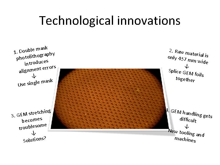
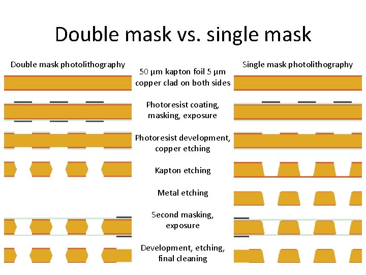
Technological innovations mask e l b u o D. 1 ography h t i l o t o h p s introduce s t error alignmen ↓ e mask Use singl etching r t s M E G 3. becomes me troubleso ↓ ? Solutions 2. Raw m aterial is only 457 mm wide ↓ Splice GE M foils together 4. GEM h andling g ets difficult ↓ New tool ing and machines

Double mask vs. single mask Double mask photolithography 50 µm kapton foil 5 µm copper clad on both sides Photoresist coating, masking, exposure Photoresist development, copper etching Kapton etching Metal etching Second masking, exposure Development, etching, final cleaning Single mask photolithography

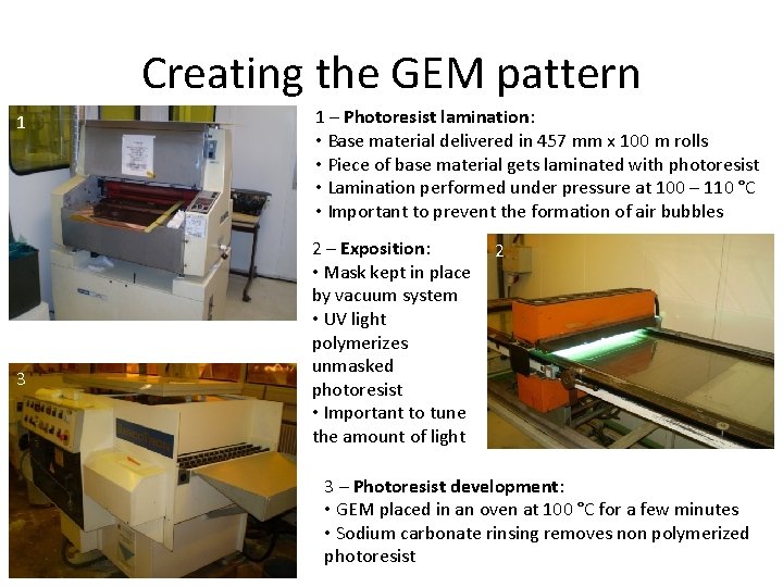
Creating the GEM pattern 1 3 1 – Photoresist lamination: • Base material delivered in 457 mm x 100 m rolls • Piece of base material gets laminated with photoresist • Lamination performed under pressure at 100 – 110 °C • Important to prevent the formation of air bubbles 2 – Exposition: • Mask kept in place by vacuum system • UV light polymerizes unmasked photoresist • Important to tune the amount of light 2 3 – Photoresist development: • GEM placed in an oven at 100 °C for a few minutes • Sodium carbonate rinsing removes non polymerized photoresist

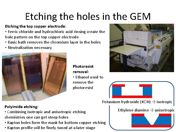
Etching the holes in the GEM Etching the top copper electrode: • Ferric chloride and hydrochloric acid rinsing create the hole pattern on the top copper electrode • Basic bath removes the chromium layer in the holes • Neutralization necessary Photoresist removal: • Ethanol used to remove the photoresist Potassium hydroxide (KOH) → isotropic Polyimide etching: • Combining isotropic and anisotropic etching chemistries one can get steep holes • Kapton holes form the mask for bottom copper etching • Kapton profile will be finely tuned at a later stage Ethylene diamine → anisotropic

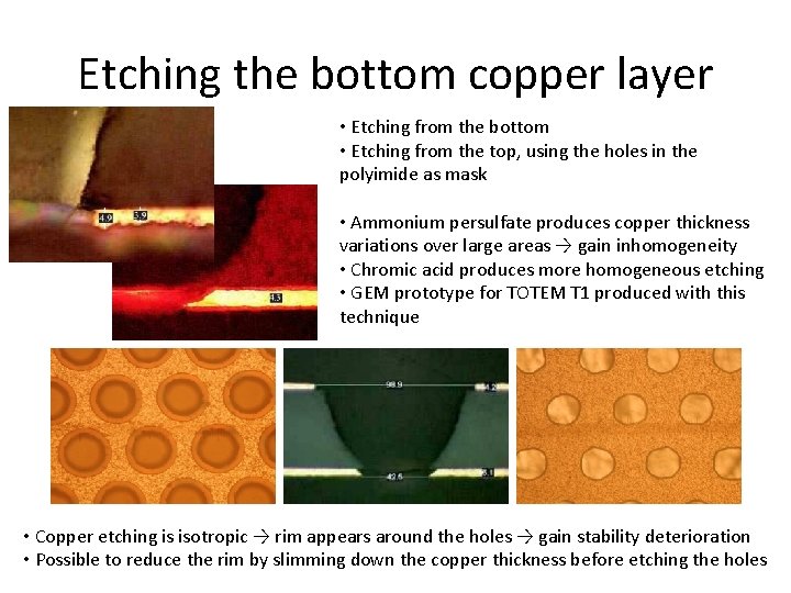
Etching the bottom copper layer • Etching from the bottom • Etching from the top, using the holes in the polyimide as mask • Ammonium persulfate produces copper thickness variations over large areas → gain inhomogeneity • Chromic acid produces more homogeneous etching • GEM prototype for TOTEM T 1 produced with this technique • Copper etching is isotropic → rim appears around the holes → gain stability deterioration • Possible to reduce the rim by slimming down the copper thickness before etching the holes

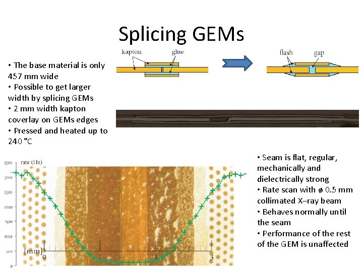
Splicing GEMs • The base material is only 457 mm wide • Possible to get larger width by splicing GEMs • 2 mm width kapton coverlay on GEMs edges • Pressed and heated up to 240 °C • Seam is flat, regular, mechanically and dielectrically strong • Rate scan with ø 0. 5 mm collimated X–ray beam • Behaves normally until the seam • Performance of the rest of the GEM is unaffected

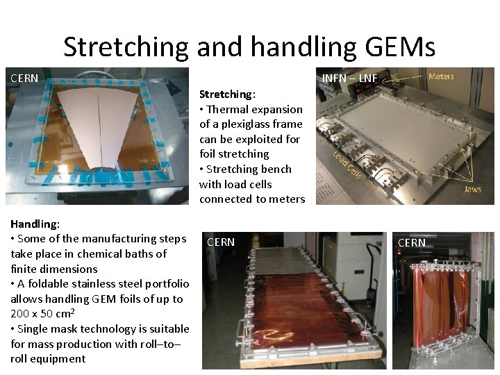
Stretching and handling GEMs CERN INFN – LNF Stretching: • Thermal expansion of a plexiglass frame can be exploited for foil stretching • Stretching bench with load cells connected to meters Handling: • Some of the manufacturing steps take place in chemical baths of finite dimensions • A foldable stainless steel portfolio allows handling GEM foils of up to 200 x 50 cm 2 • Single mask technology is suitable for mass production with roll–to– roll equipment CERN

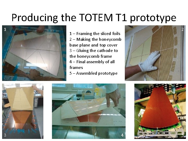
Producing the TOTEM T 1 prototype 1 3 1 – Framing the sliced foils 2 – Making the honeycomb base plane and top cover 3 – Gluing the cathode to the honeycomb frame 4 – Final assembly of all frames 5 – Assembled prototype 4 2 5

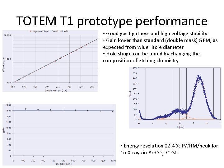
TOTEM T 1 prototype performance • Good gas tightness and high voltage stability • Gain lower than standard (double mask) GEM, as expected from wider hole diameter • Hole shape can be tuned by changing the composition of etching chemistry • Energy resolution 22. 4 % FWHM/peak for Cu X-rays in Ar: CO 2 70: 30

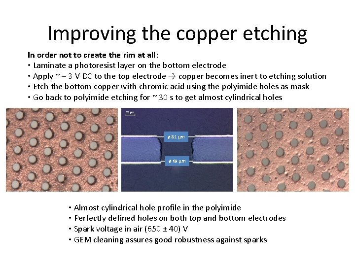
Improving the copper etching In order not to create the rim at all: • Laminate a photoresist layer on the bottom electrode • Apply ~ – 3 V DC to the top electrode → copper becomes inert to etching solution • Etch the bottom copper with chromic acid using the polyimide holes as mask • Go back to polyimide etching for ~ 30 s to get almost cylindrical holes ø 81 µm ø 69 µm • Almost cylindrical hole profile in the polyimide • Perfectly defined holes on both top and bottom electrodes • Spark voltage in air (650 ± 40) V • GEM cleaning assures good robustness against sparks

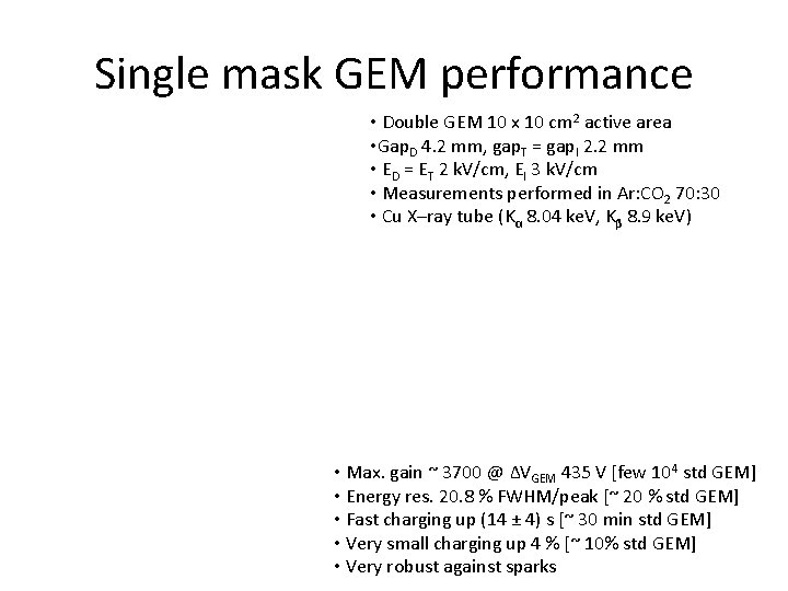
Single mask GEM performance • Double GEM 10 x 10 cm 2 active area • Gap. D 4. 2 mm, gap. T = gap. I 2. 2 mm • ED = ET 2 k. V/cm, EI 3 k. V/cm • Measurements performed in Ar: CO 2 70: 30 • Cu X–ray tube (Kα 8. 04 ke. V, Kβ 8. 9 ke. V) • Max. gain ~ 3700 @ ΔVGEM 435 V [few 104 std GEM] • Energy res. 20. 8 % FWHM/peak [~ 20 % std GEM] • Fast charging up (14 ± 4) s [~ 30 min std GEM] • Very small charging up 4 % [~ 10% std GEM] • Very robust against sparks

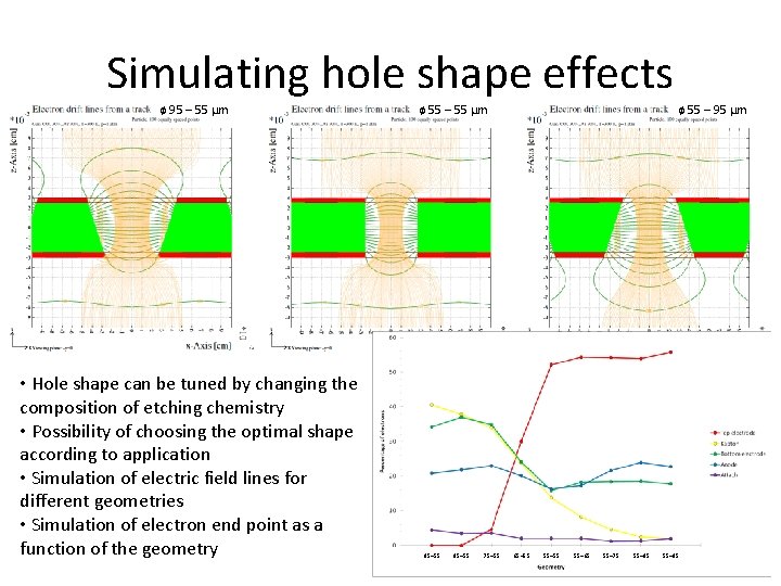
Simulating hole shape effects ø 95 – 55 µm • Hole shape can be tuned by changing the composition of etching chemistry • Possibility of choosing the optimal shape according to application • Simulation of electric field lines for different geometries • Simulation of electron end point as a function of the geometry ø 55 – 55 µm 95– 55 85– 55 75– 55 ø 55 – 95 µm 65– 55 55– 65 55– 75 55– 85 55– 95

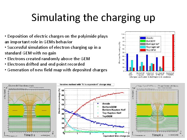
Simulating the charging up • Deposition of electric charges on the polyimide plays an important role in GEMs behavior • Successful simulation of electron charging up in a standard GEM with no gain • Electrons created randomly above the GEM • Electrons drifted and end point recorded • Generation of new field map with deposited charges Time 0 s Time 4 s

Conclusions & outlooks • The single mask technique has proven to be a valid manufacturing technology for GEMs • It was possible to build a large size triple GEM of ~ 2000 cm 2 active area which has successfully been tested • Recent refinements of the production method give better control over the hole shape • The technique offers attractive advantages for large area and large scale production • Hole parameters are under study and the optimization process is ongoing

Backup slides

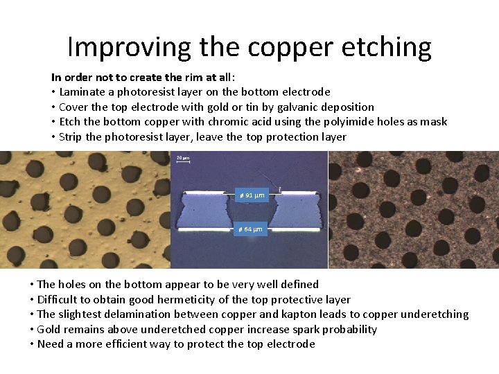
Improving the copper etching In order not to create the rim at all: • Laminate a photoresist layer on the bottom electrode • Cover the top electrode with gold or tin by galvanic deposition • Etch the bottom copper with chromic acid using the polyimide holes as mask • Strip the photoresist layer, leave the top protection layer ø 91 µm ø 64 µm • The holes on the bottom appear to be very well defined • Difficult to obtain good hermeticity of the top protective layer • The slightest delamination between copper and kapton leads to copper underetching • Gold remains above underetched copper increase spark probability • Need a more efficient way to protect the top electrode