Network Joint Research Center for Materials and Devices


- Slides: 5
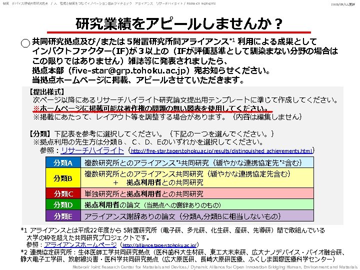
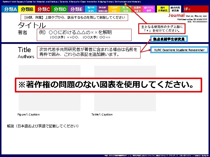
Network Joint Research Center for Materials and Devices / Dynamic Alliance for Open Innovation Bridging Human, Environment and Materials 分類B * 記載例1 多元研 IMRAM 産 研 ISIR 海外 共同研究 拠点利用 研究者 IF=6. 196 CARBON 94(2015)309 -316 グラフィン/タングステンブロンズ複合材料の創製 Published online 30 June, 2015 DOI: 10. 1016/j. carbon. 2015. 06. 072 (東北大多元研)佐藤次雄・殷シュウ・小林亮・垣花眞人、(阪大産研)関野徹、(東海大)松下純一、 (中国蘭州大)劉斌・王育華 Graphene/Mx. WO 3(M=Na, K) nanohybrids with excellent electrical properties Bin Liu, Shu Yin, Xiaoyong Wu, Yuhua Wang, Yunfang Huang, Jihuai Wu, Tohru Sekino, Junichi Matsushita, Soo Wohn Lee, Makoto Kobayashi, Masato Kakihana, Tsugio Sato ※著作権の問題のない図表を使用してください。 化学還元法によるグラフィン(r. GO)は、酸素官能基及び欠陥が多く生成されるため、その導電率は、グラフィン本来 の導電率より低くなることが多い。本研究では、グラフィンとタングステンブロンズナノ材料を複合化することで、「 並列抵抗」の様なシナージ効果により、薄膜の電気抵抗を低下(導電性を向上)させることに成功した。 Graphene (r. GO) synthesized by chemical reduction method usually shows lower conductivity than graphene original conductivity, because of the existence of many oxygen functional groups and defects. In the present research, reduction of electrical resistance (Improvement of conductivity) of the thin film was successfully realized by the synergistic “parallel resistance effect” in the graphene / tungsten bronze composites 物質・デバイス領域共同研究拠点 / 人・環境と物質をつなぐイノベーション創出ダイナミック・アライアンス リサーチハイライト / Research Highlights
Network Joint Research Center for Materials and Devices / Dynamic Alliance for Open Innovation Bridging Human, Environment and Materials 分類B 記載例2 産 研 ISIR * 先導研 拠点利用 研究者 IMCE IF=13. 858 J. Am. Chem. Soc. Vol. 139, No. 40, 14137 -14142. Published online: 7 September, 2017 DOI: 10. 1021/jacs. 7 b 06440 ブリッジ回路を搭載した超高感度電流計測システムの開発 拠点卓越学生研究員 (名大) 矢崎 啓寿・安井 隆雄・加地範匡・馬場嘉信、 (阪大産研)川合 知二、(九大先導研) 柳田 剛・長島 一樹・金井 真樹 ※ロゴや表紙などは著作権で保護されています。 Substantial Expansion of Detectable Size Range in Ionic Current Sensing through Pores by Using a Microfluidic Bridge Circuit ご利用の際は予め問題がないかご確認ください。 Hirotoshi Yasaki, Takao Yasui, Takeshi Yanagida, Noritada Kaji, Masaki Kanai, Kazuki Nagashima, NJRC Excellent Student Researcher Tomoji Kawai, Yoshinobu Baba Selected as JACS Spotlight 名大・九大・阪大など、様々なサイズ の物質を 1つの計測部で検出する検 出システムを開発 2017年 9月30日 ※著作権の問題のない図表を使用してください。 Spotlights on Recent JACS Publications ACS Contributing Correspondents J. Am. Chem. Soc. , 2017, 139 (40), pp 13959– 13959 DOI: 10. 1021/jacs. 7 b 10518 環境測定デバイス、生命科学研究、個別化医療などの分野で、効率良く物質のサイズ計測を行う方法として、近年電流 計測システムが注目されているが、様々なサイズの物質を含むサンプルを1つのサイズ規格の計測部で包括的に検出・ 分析することは原理的に困難であった。本研究では、ブリッジ回路を搭載した電流計測システムにより、微粒子・微生 物・DNA分子など広いサイズ範囲のサンプルを包括的に検出可能な超高感度電流計測システムの開発に成功した。 Ionic currents sensing system has a great promise for the electrical discrimination of various biomolecules, cells, bacteria, and viruses, however, the detectable size range has been inherently limited. In this research, we successfully demonstrated a wide range biomaterial detection system using a microfluidic bridge circuit. 物質・デバイス領域共同研究拠点 / 人・環境と物質をつなぐイノベーション創出ダイナミック・アライアンス リサーチハイライト / Research Highlights
Network Joint Research Center for Materials and Devices / Dynamic Alliance for Open Innovation Bridging Human, Environment and Materials * 分類A 記載例3 多元研 緩やかな 連携 IMRAM 共振ずり測定によるサブ 15 nm光ナノインプリント成形に 適したジアクリレートモノマーの選択 IF=3. 789 Langmuir 34, 9366 -9375 (2018) Published online: 24 July, 2018 DOI: 10. 1021/acs. langmuir. 8 b 01881 (東北大多元研) 伊東駿也・粕谷素洋・中川勝、(日立製作所) 川崎健司・鷲谷隆太・島崎譲、 (東京医科歯科大) 宮内昭浩、(東北大未来科学技術共同研究センター) 栗原和枝 Selection of Diacrylate Monomers for Sub-15 nm Ultraviolet Nanoimprinting by Resonance Shear Measurement viscous parameter (Ns m-1) Shunya Ito, Motohiro Kasuya, Kenji Kawasaki, Ryuta Washiya, Yuzuru Shimazaki, Akihiro Miyauchi, Kazue Kurihara, and Masaru Nakagawa 1000 7 nm patterning by UV nanoimprinting ※著作権の問題のない図表を使用してください。 height = 10 -11 nm height = 3 -6 nm 10 0, 1 0, 001 Figure 1 Resin pillar patterns fabricated by UV nanoimprinting using a silica mold with 7 nm diameter holes. 0 10 20 surface-surface distance (nm) Figure 2 Increase in viscosity in nano-gap between silica surfaces depending on the chemical structures of monomers. 光ナノインプリント成形おいて、サブ 15 nmサイズのパターニングに適したモノマーの選定が必要である。本研究では、 直径20, 15, 7 nmのホールパターンを有するシリカモールドを用いた光ナノインプリント成形を実証し、モノマー化学構 造の違いによる充填挙動を明らかにした。このサイズでの充填挙動は共振ずり測定により明らかにされたシリカナノ空間 中での粘度増加、および接触角測定から示されたモールド表面に対する濡れ性で説明できることを見出した。 In UV nanoimprinting, the selection of monomers suitable for sub-15 nm patterning is required. In this work, we demonstrated the patterning by UV nanoimprinting using a silica mold with 20, 15, and 7 nm diameter holes, and revealed that the monomer showing low viscosity under confinement and high wettability onto the mold surface was suitable for the patterning at this scale. 物質・デバイス領域共同研究拠点 / 人・環境と物質をつなぐイノベーション創出ダイナミック・アライアンス リサーチハイライト / Research Highlights