Multiplexer Decoder and Circuit Designing Sahar Mosleh California
- Slides: 16

Multiplexer, Decoder and Circuit Designing Sahar Mosleh California State University San Marcos Page 1

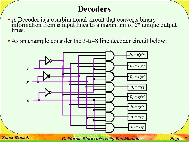
Decoders • A Decoder is a combinational circuit that converts binary information from n input lines to a maximum of 2 n unique output lines. • As an example consider the 3 -to-8 line decoder circuit below: D 0 = x’y’z’ z D 1 = x’y’z D 2 = x’yz’ y D 3 = x’yz x D 4 = xy’z’ D 5 = xy’z D 6 = xyz’ D 7 = xyz Sahar Mosleh California State University San Marcos Page 2

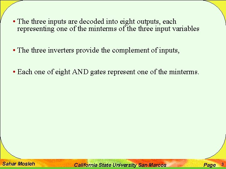
• The three inputs are decoded into eight outputs, each representing one of the minterms of the three input variables • The three inverters provide the complement of inputs, • Each one of eight AND gates represent one of the minterms. Sahar Mosleh California State University San Marcos Page 3

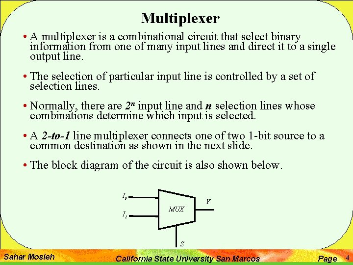
Multiplexer • A multiplexer is a combinational circuit that select binary information from one of many input lines and direct it to a single output line. • The selection of particular input line is controlled by a set of selection lines. • Normally, there are 2 n input line and n selection lines whose combinations determine which input is selected. • A 2 -to-1 line multiplexer connects one of two 1 -bit source to a common destination as shown in the next slide. • The block diagram of the circuit is also shown below. I 0 I 1 MUX Y S Sahar Mosleh California State University San Marcos Page 4

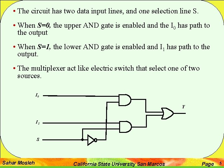
• The circuit has two data input lines, and one selection line S. • When S=0, the upper AND gate is enabled and the I 0 has path to the output • When S=1, the lower AND gate is enabled and I 1 has path to the output. • The multiplexer act like electric switch that select one of two sources. I 0 Y I 1 S Sahar Mosleh California State University San Marcos Page 5

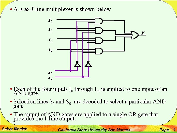
• A 4 -to-1 line multiplexer is shown below I 0 I 1 Y I 2 I 3 s 1 s 0 • Each of the four inputs I 0 through I 3, is applied to one input of an AND gate. • Selection lines S 1 and S 0 are decoded to select a particular AND gate • The output of AND gates are applied to a single OR gate that provides the 1 -line output. Sahar Mosleh California State University San Marcos Page 6

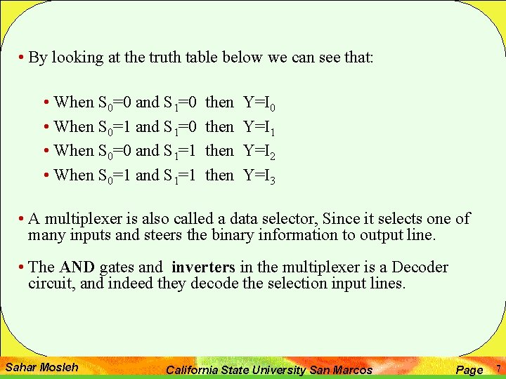
• By looking at the truth table below we can see that: • When S 0=0 and S 1=0 • When S 0=1 and S 1=0 • When S 0=0 and S 1=1 • When S 0=1 and S 1=1 then Y=I 0 Y=I 1 Y=I 2 Y=I 3 • A multiplexer is also called a data selector, Since it selects one of many inputs and steers the binary information to output line. • The AND gates and inverters in the multiplexer is a Decoder circuit, and indeed they decode the selection input lines. Sahar Mosleh California State University San Marcos Page 7

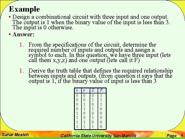
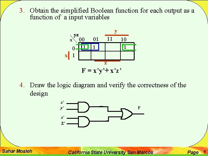
Example • Design a combinational circuit with three input and one output. The output is 1 when the binary value of the input is less than 3. The input is 0 otherwise. • Answer: 1. From the specifications of the circuit, determine the required number of inputs and outputs and assign a symbol to each. In this question, we have three input (lets call them x, y, z) and one output (lets call it F) 1. Derive the truth table that defines the required relationship between inputs and outputs. (from question it says that the output is 1, if the binary value of input is less than 3 x 0 0 1 1 Sahar Mosleh y 0 0 1 1 Z 0 1 0 1 F 1 1 1 0 0 0 California State University San Marcos Page 8

3. Obtain the simplified Boolean function for each output as a function of a input variables x yz 0 x 1 y 00 1 11 01 10 1 1 z F = x’y’+ x’z’ 4. Draw the logic diagram and verify the correctness of the design x’ y’ F x’ Z’ Sahar Mosleh California State University San Marcos Page 9

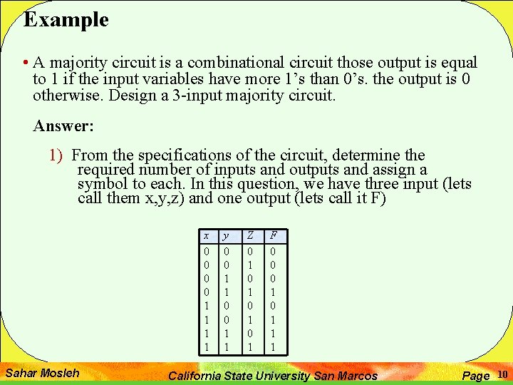
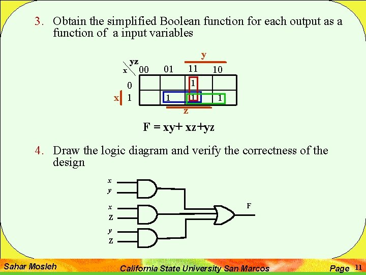
Example • A majority circuit is a combinational circuit those output is equal to 1 if the input variables have more 1’s than 0’s. the output is 0 otherwise. Design a 3 -input majority circuit. Answer: 1) From the specifications of the circuit, determine the required number of inputs and outputs and assign a symbol to each. In this question, we have three input (lets call them x, y, z) and one output (lets call it F) x 0 0 1 1 Sahar Mosleh y 0 0 1 1 Z 0 1 0 1 F 0 0 0 1 1 1 California State University San Marcos Page 10

3. Obtain the simplified Boolean function for each output as a function of a input variables x yz 0 x 1 y 00 11 01 10 1 1 z F = xy+ xz+yz 4. Draw the logic diagram and verify the correctness of the design x y x F Z y Z Sahar Mosleh California State University San Marcos Page 11

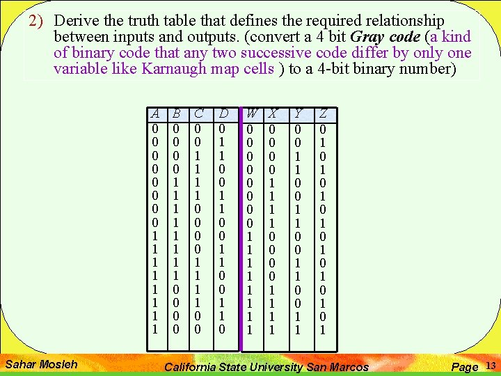
Example • Design a combinational circuit that convert a 4 bit Gray code to a 4 -bit binary number. Implement the circuit with exclusive-OR gates. A Gray Code is a kind of binary code that any two successive code differ by only one variable like Karnaugh map cells ) • Answer: 1) From the specifications of the circuit, determine the required number of inputs and outputs and assign a symbol to each. In this question we have four input (lets call them A, B, C, D) and four output (lets call them W, X, Y, Z) Sahar Mosleh California State University San Marcos Page 12

2) Derive the truth table that defines the required relationship between inputs and outputs. (convert a 4 bit Gray code (a kind of binary code that any two successive code differ by only one variable like Karnaugh map cells ) to a 4 -bit binary number) A 0 0 0 0 1 1 1 1 Sahar Mosleh B 0 0 1 1 1 1 0 0 C 0 0 1 1 1 1 0 0 D 0 1 1 0 W 0 0 0 0 1 1 1 1 X 0 0 0 0 1 1 1 1 Y 0 0 1 1 Z 0 1 0 1 California State University San Marcos Page 13

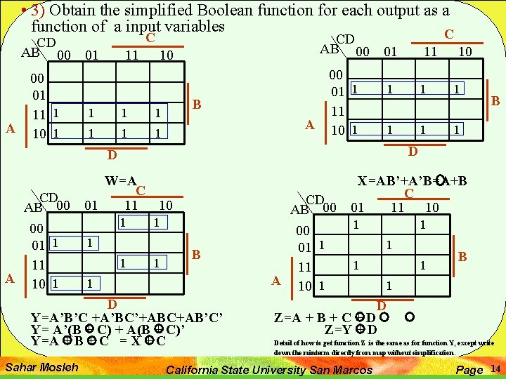
• 3) Obtain the simplified Boolean function for each output as a function of a input variables C CD AB 00 00 01 11 1 A 10 1 C 01 11 CD AB 00 10 1 1 1 B 01 11 1 1 1 00 01 1 11 A 10 1 W=A C 01 11 10 1 1 1 B 1 D Y=A’B’C +A’BC’+ABC+AB’C’ Y= A’(B + C) + A(B + C)’ Y=A + B + C = X + C Sahar Mosleh B D D CD AB 00 00 01 1 11 A 10 1 10 CD AB 00 00 01 1 11 A 10 1 X=AB’+A’B=A+B C 01 11 10 1 1 1 B 1 D Z=A + B + C + D Z=Y + D Detail of how to get function Z is the same as for function Y, except write down the minterm directly from map without simplification. California State University San Marcos Page 14

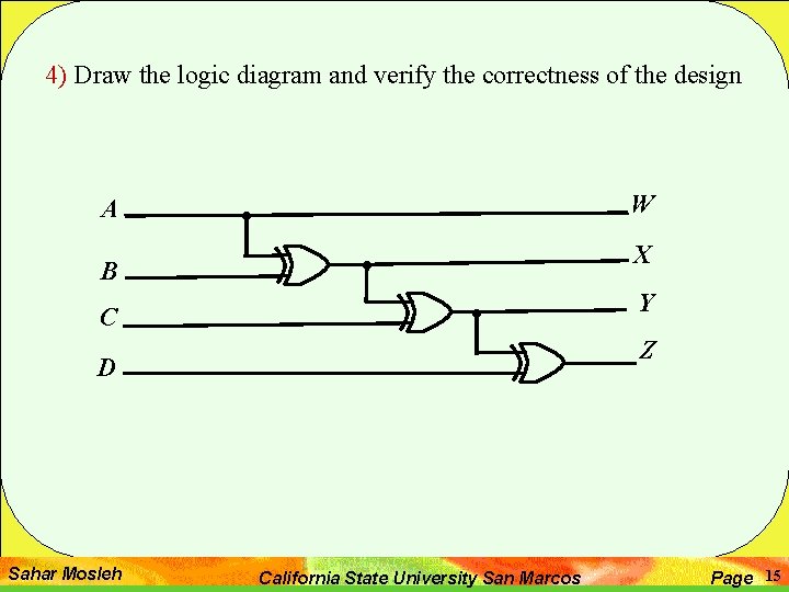
4) Draw the logic diagram and verify the correctness of the design W A X B Y C Z D Sahar Mosleh California State University San Marcos Page 15

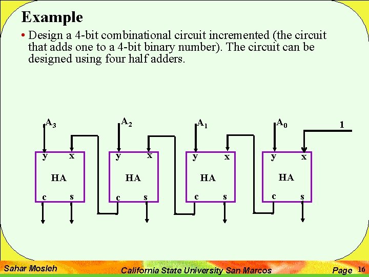
Example • Design a 4 -bit combinational circuit incremented (the circuit that adds one to a 4 -bit binary number). The circuit can be designed using four half adders. A 2 A 3 y x HA c Sahar Mosleh x y y HA s c A 0 A 1 x y c x HA HA s 1 s California State University San Marcos c s Page 16