MINTERM AND MAXTERM EXPANSIONS 350151 Digital Circuit 1
- Slides: 15

MINTERM AND MAXTERM EXPANSIONS 350151 – Digital Circuit 1 Choopan Rattanapoka

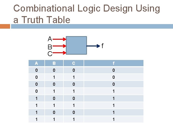
Combinational Logic Design Using a Truth Table A B C f 0 0 0 1 1 1 1 0 0 1 1 1 1 1

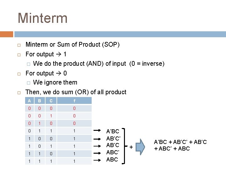
Minterm or Sum of Product (SOP) For output 1 � We do the product (AND) of input (0 = inverse) For output 0 � We ignore them Then, we do sum (OR) of all product A B C f 0 0 0 1 1 0 0 1 1 1 1 0 1 1 1 A’BC AB’C’ AB’C ABC’ ABC + A’BC + AB’C’ + AB’C + ABC’ + ABC

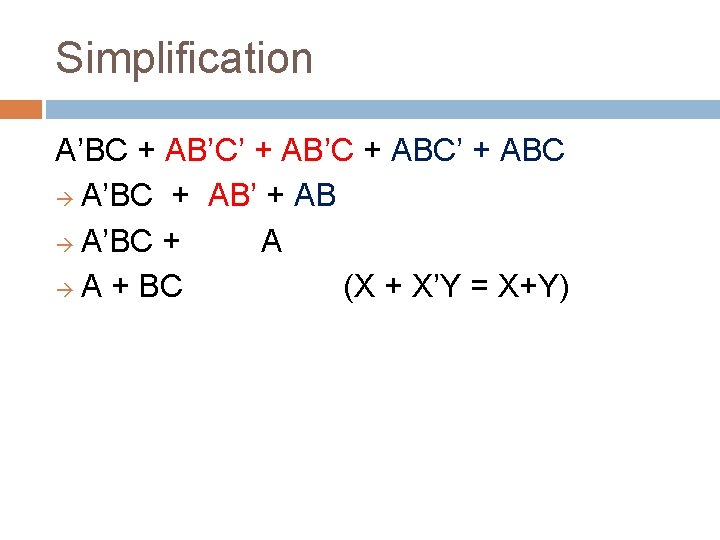
Simplification A’BC + AB’C’ + AB’C + ABC’ + ABC A’BC + AB’ + AB A’BC + A A + BC (X + X’Y = X+Y)

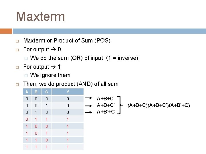
Maxterm or Product of Sum (POS) For output 0 � We do the sum (OR) of input (1 = inverse) For output 1 � We ignore them Then, we do product (AND) of all sum A B C f 0 0 0 1 1 0 0 1 1 1 1 0 1 1 1 A+B+C’ A+B’+C (A+B+C)(A+B+C’)(A+B’+C)

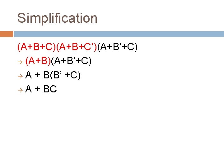
Simplification (A+B+C)(A+B+C’)(A+B’+C) (A+B)(A+B’+C) A + B(B’ +C) A + BC

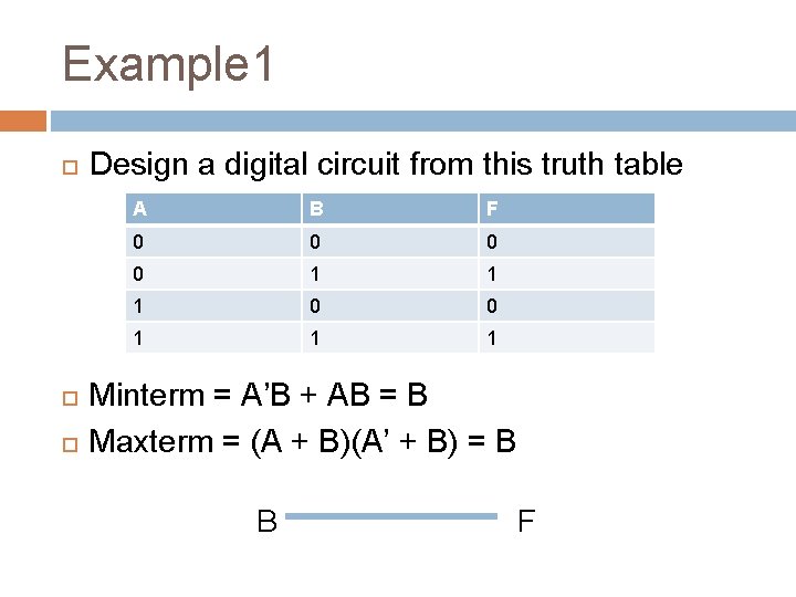
Example 1 Design a digital circuit from this truth table A B F 0 0 1 1 1 Minterm = A’B + AB = B Maxterm = (A + B)(A’ + B) = B B F

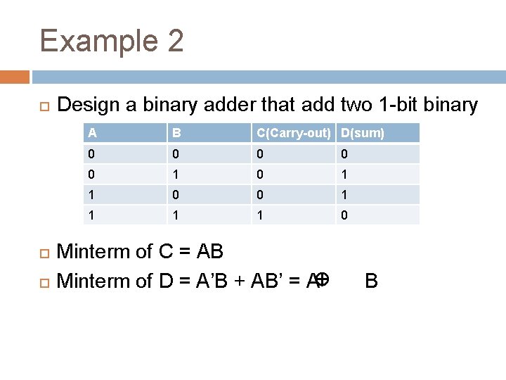
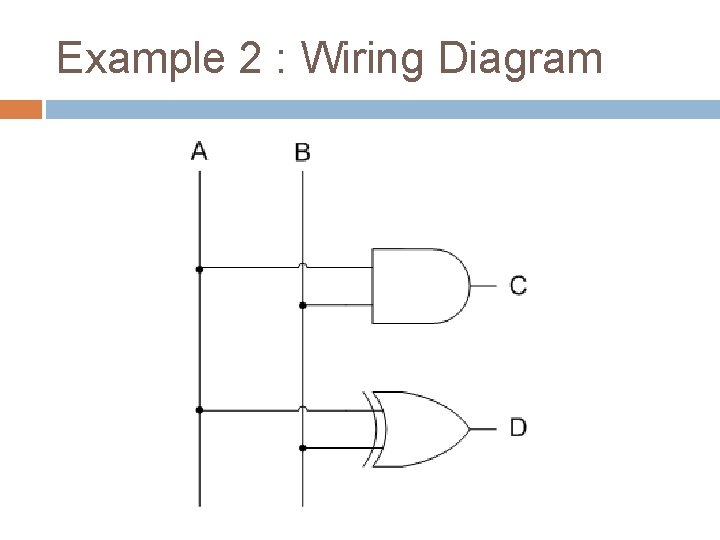
Example 2 Design a binary adder that add two 1 -bit binary A B C(Carry-out) D(sum) 0 0 0 1 1 0 Minterm of C = AB Minterm of D = A’B + AB’ = A B

Example 2 : Wiring Diagram

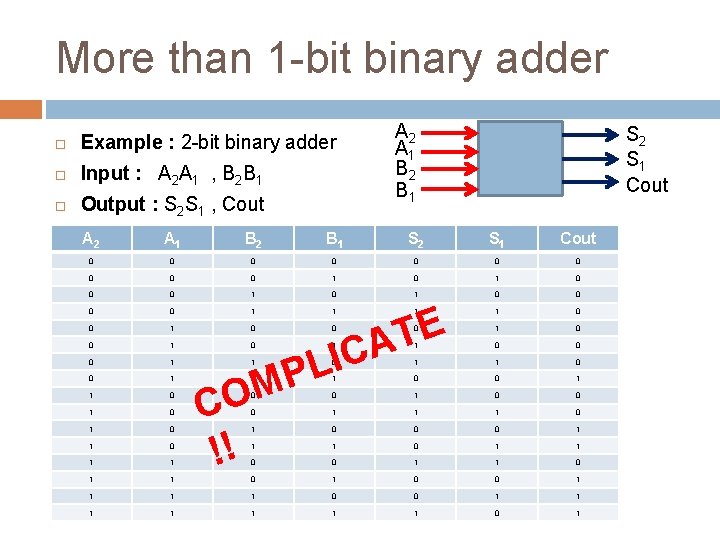
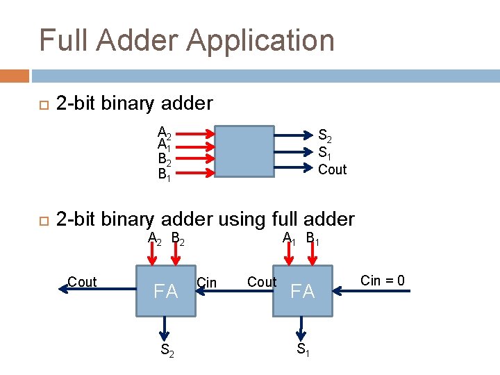
More than 1 -bit binary adder Example : 2 -bit binary adder Input : A 2 A 1 , B 2 B 1 Output : S 2 S 1 , Cout A 2 A 1 B 2 B 1 S 2 S 1 Cout 0 0 0 0 0 1 0 1 0 0 0 0 1 1 0 0 1 0 0 0 1 1 0 0 1 1 1 0 1 0 0 0 1 1 0 0 1 1 0 1 0 0 1 1 1 1 1 0 1 M O C !! I L P 1 0 E T CA 1 0 1

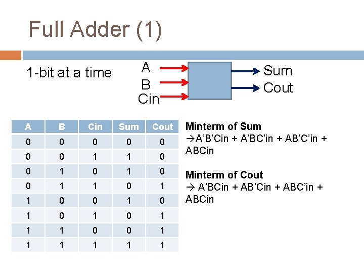
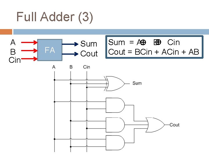
Full Adder (1) A B Cin 1 -bit at a time Sum Cout A B Cin Sum Cout 0 0 0 0 1 1 0 0 1 0 1 1 1 0 0 1 1 1 Minterm of Sum A’B’Cin + A’BC’in + AB’C’in + ABCin Minterm of Cout A’BCin + AB’Cin + ABC’in + ABCin

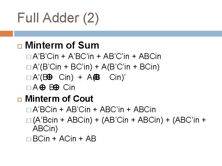
Full Adder (2) Minterm of Sum � A’B’Cin + A’BC’in + AB’C’in + ABCin � A’(B’Cin + BC’in) + A(B’C’in + BCin) � A’(B Cin) + A(B Cin)’ �A B Cin Minterm of Cout � A’BCin + AB’Cin + ABC’in + ABCin � (A’Bcin + ABCin) + (AB’Cin + ABCin) + (ABC’in + ABCin) � BCin + AB

Full Adder (3) A B Cin FA Sum Cout Sum = A B Cin Cout = BCin + AB

Full Adder Application 2 -bit binary adder A 2 A 1 B 2 B 1 S 2 S 1 Cout 2 -bit binary adder using full adder A 2 B 2 Cout FA S 2 A 1 B 1 Cin Cout FA S 1 Cin = 0

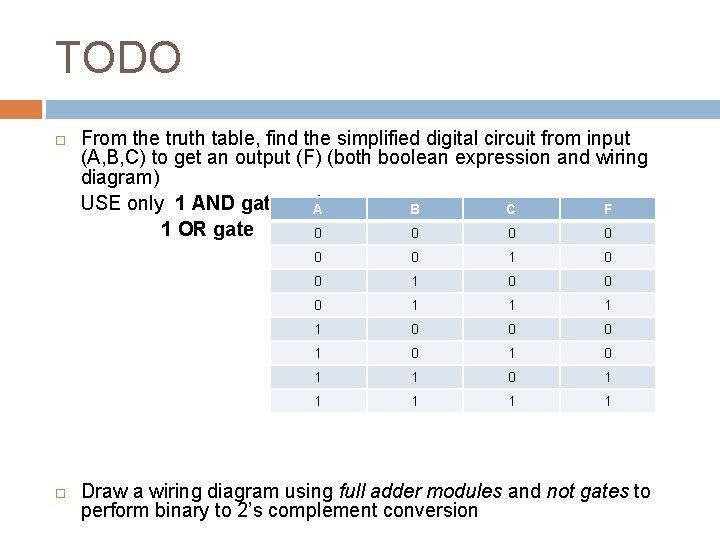
TODO From the truth table, find the simplified digital circuit from input (A, B, C) to get an output (F) (both boolean expression and wiring diagram) USE only 1 AND gate and. A B C F 1 OR gate 0 0 0 1 1 0 0 0 1 0 1 1 1 1 1 Draw a wiring diagram using full adder modules and not gates to perform binary to 2’s complement conversion