Layout Considerations of NonIsolated Switching Mode Power Supply






- Slides: 28
Layout Considerations of Non-Isolated Switching Mode Power Supply Presented by Henry Zhang Power Business Unit Linear Technology Corp. Oct. 2003 Henry J. Zhang, Oct. 2003 FAE Meeting LTC Company Confidential Hzhang@linear. com, 3863
1. General Discussion Henry J. Zhang, Oct. 2003 FAE Meeting LTC Company Confidential Hzhang@linear. com, 3863
Plan of the Power Supply Layout • In the system, power supply should be close to its load devices. • Cooling fan should be close to the supply to limit its component thermal stress. • Select the right number of layers and copper thickness • The large size passive components (inductors, bulk capacitors) should not block air flow to power MOSFETs • Power supply designer should always works closely with PCB designer on the critical layout design Henry J. Zhang, Oct. 2003 FAE Meeting LTC Company Confidential Hzhang@linear. com, 3863
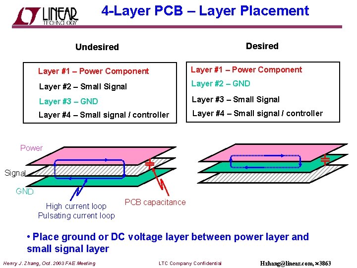
4 -Layer PCB – Layer Placement Desired Undesired Layer #1 – Power Component Layer #2 – Small Signal Layer #2 – GND Layer #3 – Small Signal Layer #4 – Small signal / controller Power Signal GND High current loop Pulsating current loop PCB capacitance • Place ground or DC voltage layer between power layer and small signal layer Henry J. Zhang, Oct. 2003 FAE Meeting LTC Company Confidential Hzhang@linear. com, 3863
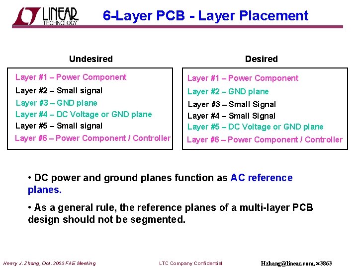
6 -Layer PCB - Layer Placement Undesired Desired Layer #1 – Power Component Layer #2 – Small signal Layer #2 – GND plane Layer #3 – GND plane Layer #4 – DC Voltage or GND plane Layer #5 – Small signal Layer #3 – Small Signal Layer #4 – Small Signal Layer #5 – DC Voltage or GND plane Layer #6 – Power Component / Controller • DC power and ground planes function as AC reference planes. • As a general rule, the reference planes of a multi-layer PCB design should not be segmented. Henry J. Zhang, Oct. 2003 FAE Meeting LTC Company Confidential Hzhang@linear. com, 3863
Small Signal Traces on Reference Layer • If the small signal traces have to be routed on the reference layer, use short traces with proper direction: Desired Reference Layer Undesired Reference Layer current PWM IC Coupled AC current return path Henry J. Zhang, Oct. 2003 FAE Meeting MOSFET LTC Company Confidential Hzhang@linear. com, 3863
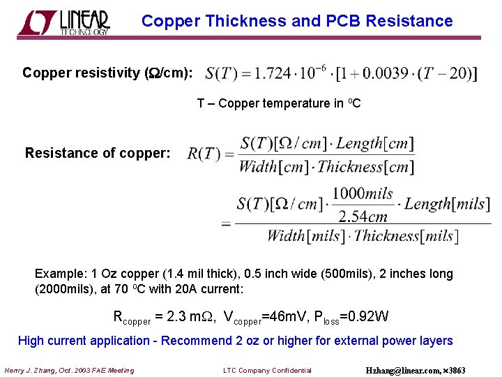
Copper Thickness and PCB Resistance Copper resistivity ( /cm): T – Copper temperature in o. C Resistance of copper: Example: 1 Oz copper (1. 4 mil thick), 0. 5 inch wide (500 mils), 2 inches long (2000 mils), at 70 o. C with 20 A current: Rcopper = 2. 3 m , Vcopper=46 m. V, Ploss=0. 92 W High current application - Recommend 2 oz or higher for external power layers Henry J. Zhang, Oct. 2003 FAE Meeting LTC Company Confidential Hzhang@linear. com, 3863
2. DC/DC Converter Power Stage Layout Henry J. Zhang, Oct. 2003 FAE Meeting LTC Company Confidential Hzhang@linear. com, 3863
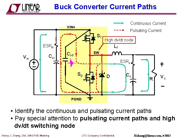
Buck Converter Current Paths Continuous Current VIN+ Pulsating Current ST High dv/dt node ESRin Vin Cin LF SW CHF ESRo SB D Co R Vo PGND • Identify the continuous and pulsating current paths • Pay special attention to pulsating current paths and high dv/dt switching node Henry J. Zhang, Oct. 2003 FAE Meeting LTC Company Confidential Hzhang@linear. com, 3863
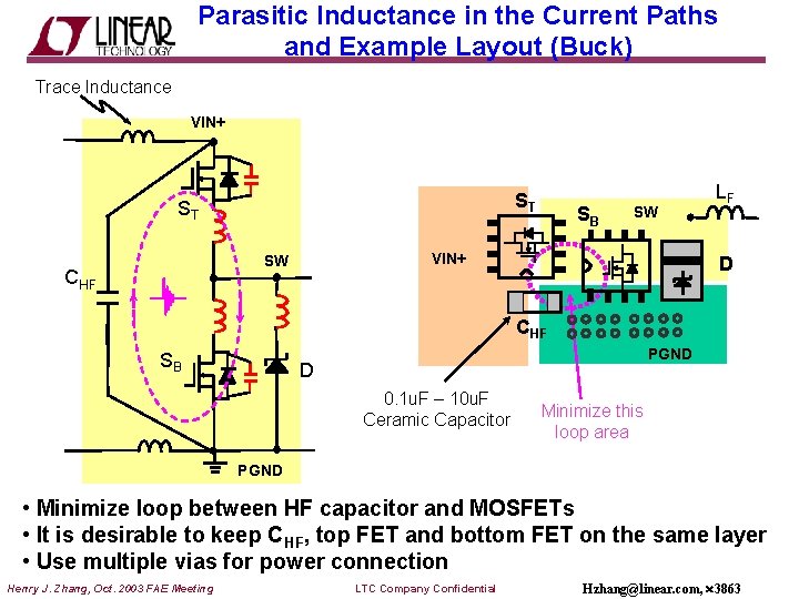
Parasitic Inductance in the Current Paths and Example Layout (Buck) Trace Inductance VIN+ ST ST SW VIN+ SW CHF SB LF D CHF SB PGND D 0. 1 u. F – 10 u. F Ceramic Capacitor Minimize this loop area PGND • Minimize loop between HF capacitor and MOSFETs • It is desirable to keep CHF, top FET and bottom FET on the same layer • Use multiple vias for power connection Henry J. Zhang, Oct. 2003 FAE Meeting LTC Company Confidential Hzhang@linear. com, 3863
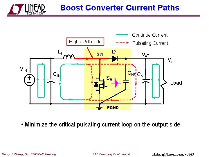
Boost Converter Current Paths Continue Current High dv/dt node LF VIN CIN SW Pulsating Current D SB Vo + CHF C Vo o Load PGND • Minimize the critical pulsating current loop on the output side Henry J. Zhang, Oct. 2003 FAE Meeting LTC Company Confidential Hzhang@linear. com, 3863
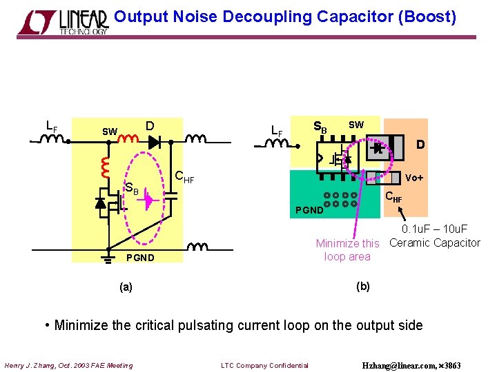
Output Noise Decoupling Capacitor (Boost) LF D SW SB SB LF SW D CHF Vo+ CHF PGND 0. 1 u. F – 10 u. F Minimize this Ceramic Capacitor loop area PGND (b) (a) • Minimize the critical pulsating current loop on the output side Henry J. Zhang, Oct. 2003 FAE Meeting LTC Company Confidential Hzhang@linear. com, 3863
12 V-to-2. 5 V/30 A LTC 3729 Supply Layout Example VIN+ (12 V) VO+ (2. 5 V) LF 1 QT CIN SW 1 LTC 3729 Co QB GND Co SW 2 VIN+ VO+ (2. 5 V) (a) Henry J. Zhang, Oct. 2003 FAE Meeting LTC Company Confidential Hzhang@linear. com, 3863
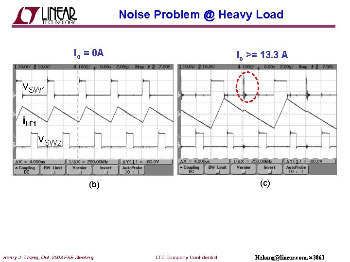
Noise Problem @ Heavy Load Io = 0 A Io >= 13. 3 A v. SW 1 i. LF 1 v. SW 2 (c) (b) Henry J. Zhang, Oct. 2003 FAE Meeting LTC Company Confidential Hzhang@linear. com, 3863
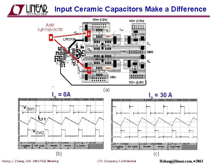
Input Ceramic Capacitors Make a Difference Add 1 u. F/16 V/X 7 R Io = 0 A (a) Io = 30 A v. SW 1 i. LF 1 v. SW 2 (b) Henry J. Zhang, Oct. 2003 FAE Meeting (c) LTC Company Confidential Hzhang@linear. com, 3863
Land Patterns of Power Components Desired Undesired - + R/C/D/L C - + C R/C/D/L FET Connected Via • Use wide / short copper trace for power components • Use multiple vias for inter-layer connections • Avoid improper use of “thermal relief” • Minimize resistance and inductance Henry J. Zhang, Oct. 2003 FAE Meeting LTC Company Confidential Hzhang@linear. com, 3863
3. 3 V/40 A LTC 3729 Layout Design Example High Current Trace Henry J. Zhang, Oct. 2003 FAE Meeting LTC Company Confidential Hzhang@linear. com, 3863
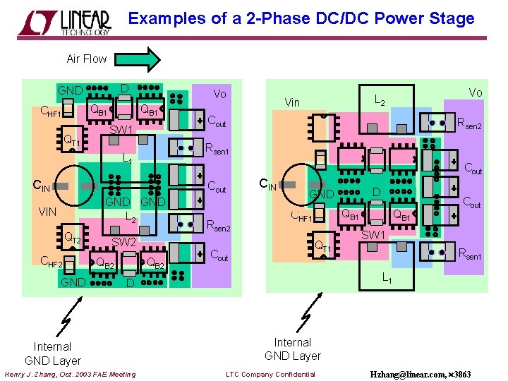
Examples of a 2 -Phase DC/DC Power Stage Air Flow D GND QB 1 CHF 1 QT 1 Vo QB 1 SW 1 Cout CIN Cout GND L 2 QT 2 CHF 2 GND SW 2 QB 2 Rsen 1 L 1 VIN Rsen 2 Cout CIN Henry J. Zhang, Oct. 2003 FAE Meeting D GND QB 1 CHF 1 QT 1 QB 1 Cout SW 1 Rsen 1 L 1 D Internal GND Layer Vo L 2 Vin Internal GND Layer LTC Company Confidential Hzhang@linear. com, 3863
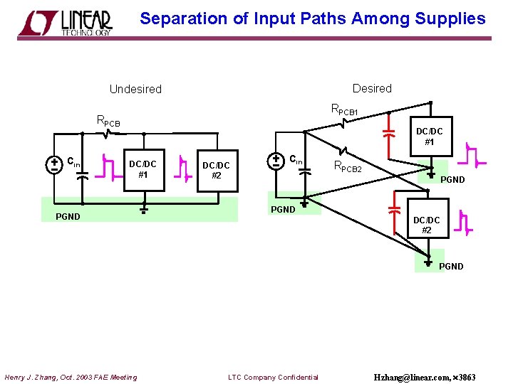
Separation of Input Paths Among Supplies Desired Undesired RPCB 1 RPCB Cin DC/DC #1 PGND DC/DC #2 Cin RPCB 2 PGND DC/DC #2 PGND Henry J. Zhang, Oct. 2003 FAE Meeting LTC Company Confidential Hzhang@linear. com, 3863
3. Layout of the Controller and MOSFET Drivers Henry J. Zhang, Oct. 2003 FAE Meeting LTC Company Confidential Hzhang@linear. com, 3863
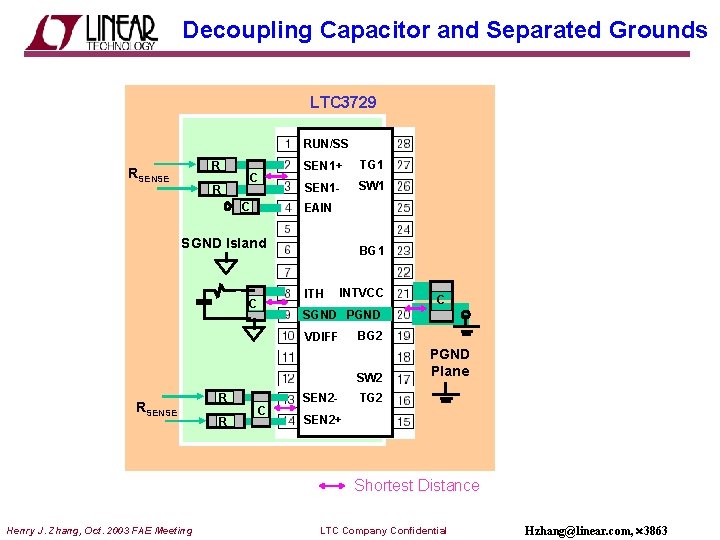
Decoupling Capacitor and Separated Grounds LTC 3729 RUN/SS R RSENSE R C C SEN 1+ TG 1 SEN 1 - SW 1 EAIN SGND Island C BG 1 ITH INTVCC VDIFF BG 2 SW 2 RSENSE R R C C SGND PGND SEN 2 - PGND Plane TG 2 SEN 2+ Shortest Distance Henry J. Zhang, Oct. 2003 FAE Meeting LTC Company Confidential Hzhang@linear. com, 3863
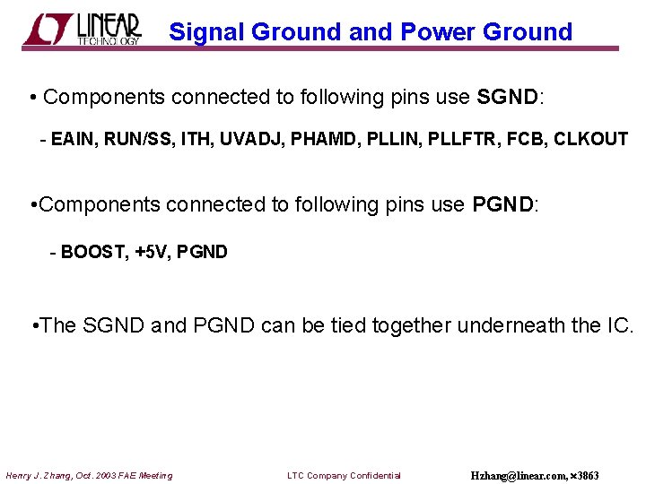
Signal Ground and Power Ground • Components connected to following pins use SGND: - EAIN, RUN/SS, ITH, UVADJ, PHAMD, PLLIN, PLLFTR, FCB, CLKOUT • Components connected to following pins use PGND: - BOOST, +5 V, PGND • The SGND and PGND can be tied together underneath the IC. Henry J. Zhang, Oct. 2003 FAE Meeting LTC Company Confidential Hzhang@linear. com, 3863
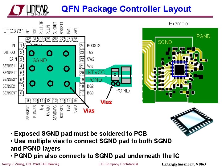
QFN Package Controller Layout Example LTC 3731 PGND SGND INTVCC C PGND Vias • Exposed SGND pad must be soldered to PCB • Use multiple vias to connect SGND pad to both SGND and PGND layers • PGND pin also connects to SGND pad underneath the IC Henry J. Zhang, Oct. 2003 FAE Meeting LTC Company Confidential Hzhang@linear. com, 3863
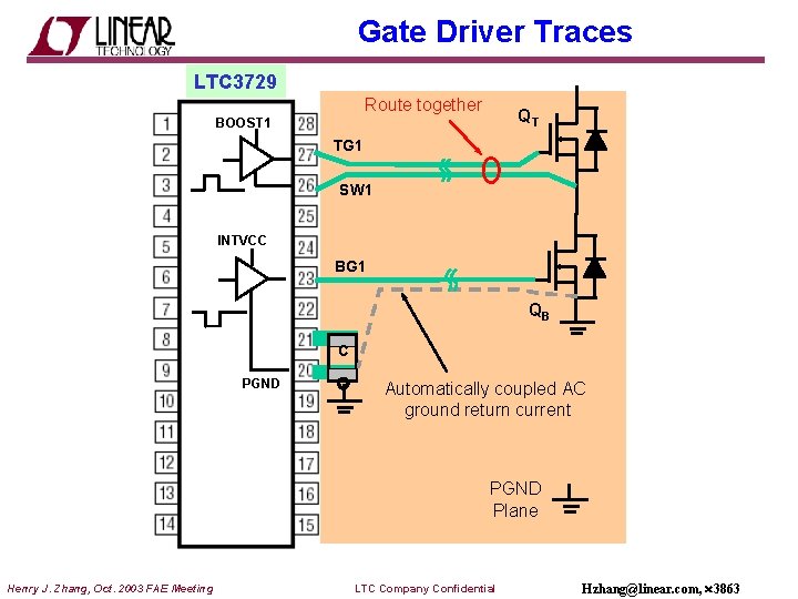
Gate Driver Traces LTC 3729 Route together QT BOOST 1 TG 1 SW 1 INTVCC BG 1 QB C PGND Automatically coupled AC ground return current PGND Plane Henry J. Zhang, Oct. 2003 FAE Meeting LTC Company Confidential Hzhang@linear. com, 3863
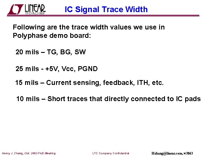
IC Signal Trace Width Following are the trace width values we use in Polyphase demo board: 20 mils – TG, BG, SW 25 mils - +5 V, Vcc, PGND 15 mils – Current sensing, feedback, ITH, etc. 10 mils – Short traces that directly connected to IC pads Henry J. Zhang, Oct. 2003 FAE Meeting LTC Company Confidential Hzhang@linear. com, 3863
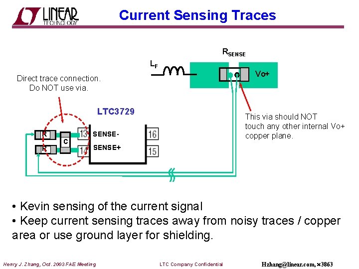
Current Sensing Traces RSENSE LF Vo+ Direct trace connection. Do NOT use via. LTC 3729 R R This via should NOT touch any other internal Vo+ copper plane. SENSEC SENSE+ • Kevin sensing of the current signal • Keep current sensing traces away from noisy traces / copper area or use ground layer for shielding. Henry J. Zhang, Oct. 2003 FAE Meeting LTC Company Confidential Hzhang@linear. com, 3863
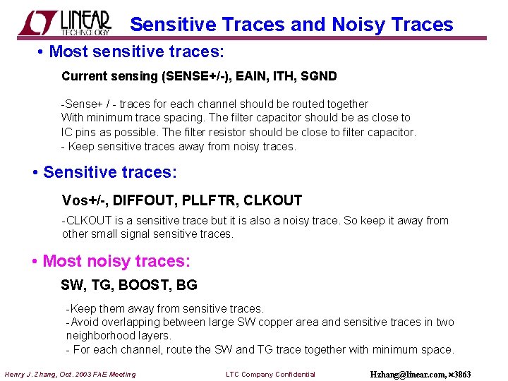
Sensitive Traces and Noisy Traces • Most sensitive traces: Current sensing (SENSE+/-), EAIN, ITH, SGND -Sense+ / - traces for each channel should be routed together With minimum trace spacing. The filter capacitor should be as close to IC pins as possible. The filter resistor should be close to filter capacitor. - Keep sensitive traces away from noisy traces. • Sensitive traces: Vos+/-, DIFFOUT, PLLFTR, CLKOUT -CLKOUT is a sensitive trace but it is also a noisy trace. So keep it away from other small signal sensitive traces. • Most noisy traces: SW, TG, BOOST, BG -Keep them away from sensitive traces. -Avoid overlapping between large SW copper area and sensitive traces in two neighborhood layers. - For each channel, route the SW and TG trace together with minimum space. Henry J. Zhang, Oct. 2003 FAE Meeting LTC Company Confidential Hzhang@linear. com, 3863
Summary - Layout Checklist • Plan of the layout: – Location of the supply / load / bulk capacitors – # of layers / layer placement / copper thickness • Power stage layout: – Power component placement – Power component land patterns – Identify pulsating current paths – Decouple capacitor close to MOSFET – Short / wide copper trace and multiple vias for high current • Controller circuit layout: – Decoupling capacitors close to pins – Separate signal / power grounds – Current sensing – De-couple sensitive and noisy traces – Gate driver traces – Select proper trace width Henry J. Zhang, Oct. 2003 FAE Meeting LTC Company Confidential Hzhang@linear. com, 3863