CS 161 Ch 7 Memory Hierarchy LECTURE 22

- Slides: 15
CS 161 Ch 7: Memory Hierarchy LECTURE 22 Instructor: L. N. Bhuyan www. cs. ucr. edu/~bhuyan 1 1999 ©UCB
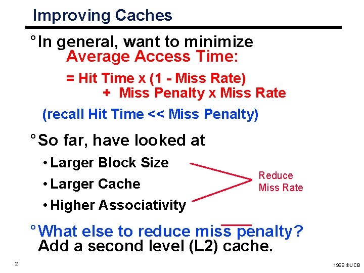
Improving Caches ° In general, want to minimize Average Access Time: = Hit Time x (1 - Miss Rate) + Miss Penalty x Miss Rate (recall Hit Time << Miss Penalty) ° So far, have looked at • Larger Block Size • Larger Cache • Higher Associativity Reduce Miss Rate ° What else to reduce miss penalty? Add a second level (L 2) cache. 2 1999 ©UCB
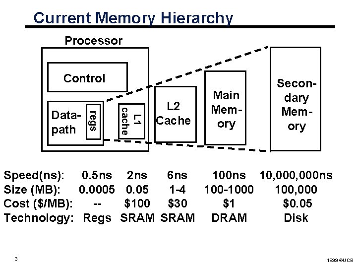
Current Memory Hierarchy Processor Control L 1 cache regs Datapath L 2 Cache Main Memory Secondary Memory Speed(ns): 0. 5 ns 2 ns 6 ns 100 ns 10, 000 ns Size (MB): 0. 0005 0. 05 1 -4 100 -1000 100, 000 Cost ($/MB): -$100 $30 $1 $0. 05 Technology: Regs SRAM DRAM Disk 3 1999 ©UCB
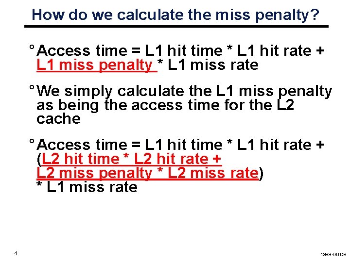
How do we calculate the miss penalty? ° Access time = L 1 hit time * L 1 hit rate + L 1 miss penalty * L 1 miss rate ° We simply calculate the L 1 miss penalty as being the access time for the L 2 cache ° Access time = L 1 hit time * L 1 hit rate + (L 2 hit time * L 2 hit rate + L 2 miss penalty * L 2 miss rate) * L 1 miss rate 4 1999 ©UCB
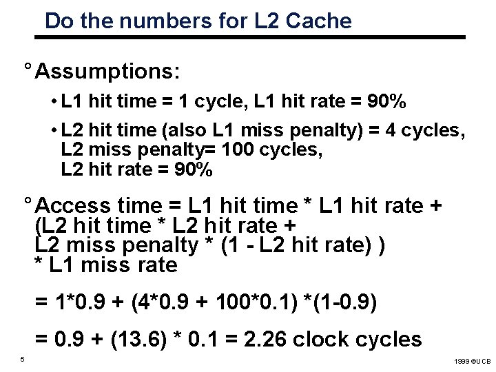
Do the numbers for L 2 Cache ° Assumptions: • L 1 hit time = 1 cycle, L 1 hit rate = 90% • L 2 hit time (also L 1 miss penalty) = 4 cycles, L 2 miss penalty= 100 cycles, L 2 hit rate = 90% ° Access time = L 1 hit time * L 1 hit rate + (L 2 hit time * L 2 hit rate + L 2 miss penalty * (1 - L 2 hit rate) ) * L 1 miss rate = 1*0. 9 + (4*0. 9 + 100*0. 1) *(1 -0. 9) = 0. 9 + (13. 6) * 0. 1 = 2. 26 clock cycles 5 1999 ©UCB
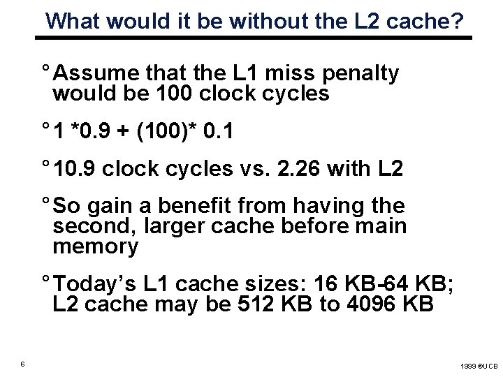
What would it be without the L 2 cache? ° Assume that the L 1 miss penalty would be 100 clock cycles ° 1 *0. 9 + (100)* 0. 1 ° 10. 9 clock cycles vs. 2. 26 with L 2 ° So gain a benefit from having the second, larger cache before main memory ° Today’s L 1 cache sizes: 16 KB-64 KB; L 2 cache may be 512 KB to 4096 KB 6 1999 ©UCB
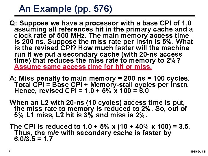
An Example (pp. 576) Q: Suppose we have a processor with a base CPI of 1. 0 assuming all references hit in the primary cache and a clock rate of 500 MHz. The main memory access time is 200 ns. Suppose the miss rate per instn is 5%. What is the revised CPI? How much faster will the machine run if we put a secondary cache (with 20 -ns access time) that reduces the miss rate to memory to 2%? Assume same access time for hit or miss. A: Miss penalty to main memory = 200 ns = 100 cycles. Total CPI = Base CPI + Memory-stall cycles per instn. Hence, revised CPI = 1. 0 + 5% x 100 = 6. 0 When an L 2 with 20 -ns (10 cycles) access time is put, the miss rate to memory is reduced to 2%. So, out of 5% L 1 miss, L 2 hit is 3% and miss is 2%. The CPI is reduced to 1. 0 + 5% x (10 + 40% x 100) = 3. 5. Thus, the m/c with secondary cache is faster by 6. 0/3. 5 = 1. 7 7 1999 ©UCB
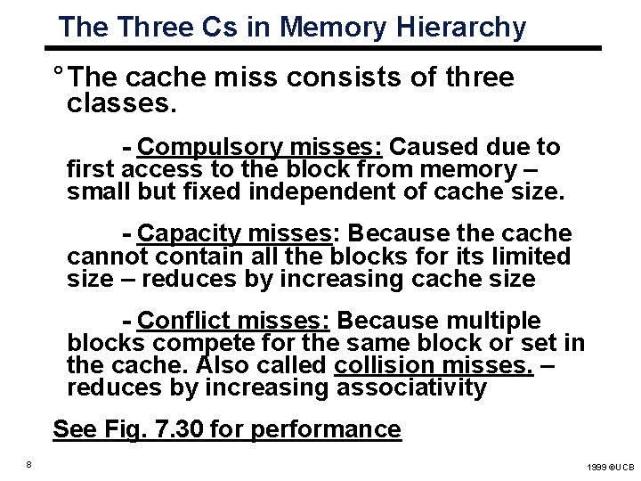
The Three Cs in Memory Hierarchy ° The cache miss consists of three classes. - Compulsory misses: Caused due to first access to the block from memory – small but fixed independent of cache size. - Capacity misses: Because the cache cannot contain all the blocks for its limited size – reduces by increasing cache size - Conflict misses: Because multiple blocks compete for the same block or set in the cache. Also called collision misses. – reduces by increasing associativity See Fig. 7. 30 for performance 8 1999 ©UCB
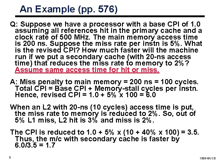
An Example (pp. 576) Q: Suppose we have a processor with a base CPI of 1. 0 assuming all references hit in the primary cache and a clock rate of 500 MHz. The main memory access time is 200 ns. Suppose the miss rate per instn is 5%. What is the revised CPI? How much faster will the machine run if we put a secondary cache (with 20 -ns access time) that reduces the miss rate to memory to 2%? Assume same access time for hit or miss. A: Miss penalty to main memory = 200 ns = 100 cycles. Total CPI = Base CPI + Memory-stall cycles per instn. Hence, revised CPI = 1. 0 + 5% x 100 = 6. 0 When an L 2 with 20 -ns (10 cycles) access time is put, the miss rate to memory is reduced to 2%. So, out of 5% L 1 miss, L 2 hit is 3% and miss is 2%. The CPI is reduced to 1. 0 + 5% x (10 + 40% x 100) = 3. 5. Thus, the m/c with secondary cache is faster by 6. 0/3. 5 = 1. 7 9 1999 ©UCB
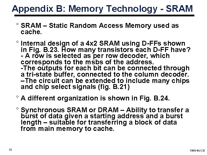
Appendix B: Memory Technology - SRAM ° SRAM – Static Random Access Memory used as cache. ° Internal design of a 4 x 2 SRAM using D-FFs shown in Fig. B. 23. How many transistors each D-FF have? - A row is selected as per row decoder, which corresponds to the msbs of the address. -The outputs for each bit can be connected through a tri-state buffer, connected to the column decoder. –The circuit can be extended to include many chips and chip select signals (fig. B. 21) ° A different organization is shown in Fig. B. 24. ° Synchronous SRAM or DRAM – Ability to transfer a burst of data given a starting address and a burst length – suitable for transferring a block of data from main memory to cache. 10 1999 ©UCB
Figs. B. 23 and B. 24 (Appendix B) Read SRAM from pp. B-26 through B-30 Figs B. 21, B. 22, B. 23 and B. 24 11 1999 ©UCB
Dynamic Random Access Memory - DRAM ° DRAM organization is similar to SRAM except that each bit of DRAM is constructed using a pass transistor and a capacitor, shown in Fig. B. 25 ° Less number of transistors/bit gives high density, but slow discharge through capacitor. ° Capacitor needs to be recharged or refreshed giving rise to high cycle time. ° Uses a two-level decoder as shown in Fig. B. 26. Note that 2048 bits are accessed per row, but only one bit is used. ° Page-mode DRAM – Why not use these bits without row access by changing column address only? ° Nibble-mode RAM – provides 4 bits (nibble) for every row access 12 1999 ©UCB
Figs. B. 25 and B. 26 (Appendix B) ° Read DRAM pp. B-31 to B-33 ° Understand Figs. B. 25 and B. 26 13 1999 ©UCB
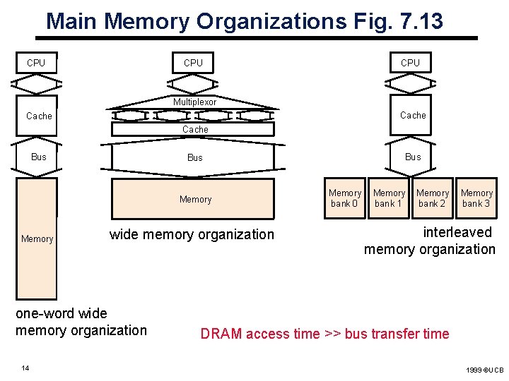
Main Memory Organizations Fig. 7. 13 CPU CPU Multiplexor Cache Bus Memory wide memory organization one-word wide memory organization 14 Bus Memory bank 0 Memory bank 1 Memory bank 2 Memory bank 3 interleaved memory organization DRAM access time >> bus transfer time 1999 ©UCB
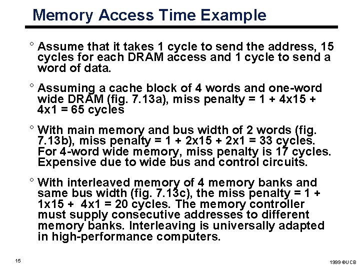
Memory Access Time Example ° Assume that it takes 1 cycle to send the address, 15 cycles for each DRAM access and 1 cycle to send a word of data. ° Assuming a cache block of 4 words and one-word wide DRAM (fig. 7. 13 a), miss penalty = 1 + 4 x 15 + 4 x 1 = 65 cycles ° With main memory and bus width of 2 words (fig. 7. 13 b), miss penalty = 1 + 2 x 15 + 2 x 1 = 33 cycles. For 4 -word wide memory, miss penalty is 17 cycles. Expensive due to wide bus and control circuits. ° With interleaved memory of 4 memory banks and same bus width (fig. 7. 13 c), the miss penalty = 1 + 1 x 15 + 4 x 1 = 20 cycles. The memory controller must supply consecutive addresses to different memory banks. Interleaving is universally adapted in high-performance computers. 15 1999 ©UCB