Computer Design Project ELEC 52006200 Computer Architecture and

- Slides: 15

Computer Design Project ELEC 5200/6200 -Computer Architecture and Design Fall 2007 Vishwani D. Agrawal James J. Danaher Professor Department of Electrical and Computer Engineering Auburn University, Auburn, AL 36849. http: //www. eng. auburn. edu/~vagrawal@eng. auburn. edu Aug. 24, 2007 ELEC 5200/6200 Project 1

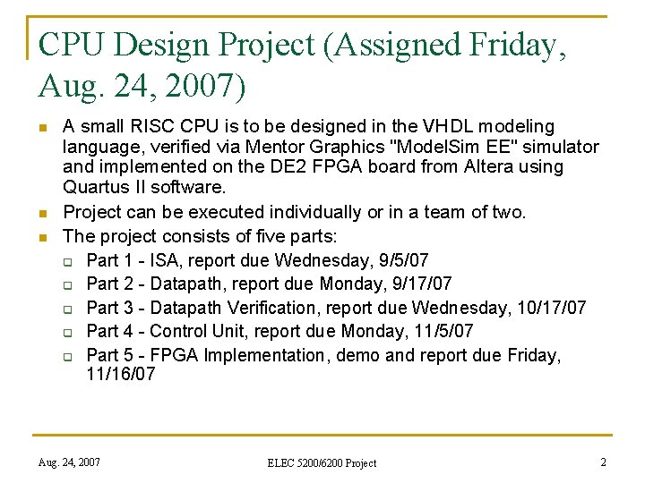
CPU Design Project (Assigned Friday, Aug. 24, 2007) n n n A small RISC CPU is to be designed in the VHDL modeling language, verified via Mentor Graphics "Model. Sim EE" simulator and implemented on the DE 2 FPGA board from Altera using Quartus II software. Project can be executed individually or in a team of two. The project consists of five parts: q Part 1 - ISA, report due Wednesday, 9/5/07 q Part 2 - Datapath, report due Monday, 9/17/07 q Part 3 - Datapath Verification, report due Wednesday, 10/17/07 q Part 4 - Control Unit, report due Monday, 11/5/07 q Part 5 - FPGA Implementation, demo and report due Friday, 11/16/07 Aug. 24, 2007 ELEC 5200/6200 Project 2

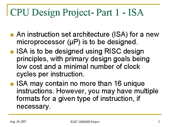
CPU Design Project- Part 1 - ISA n n n An instruction set architecture (ISA) for a new microprocessor (μP) is to be designed. ISA is to be designed using RISC design principles, with primary design goals being low cost and a minimal number of clock cycles per instruction. ISA may contain no more than 16 unique instructions. However, you may have multiple formats for a given type of instruction, if necessary. Aug. 24, 2007 ELEC 5200/6200 Project 3

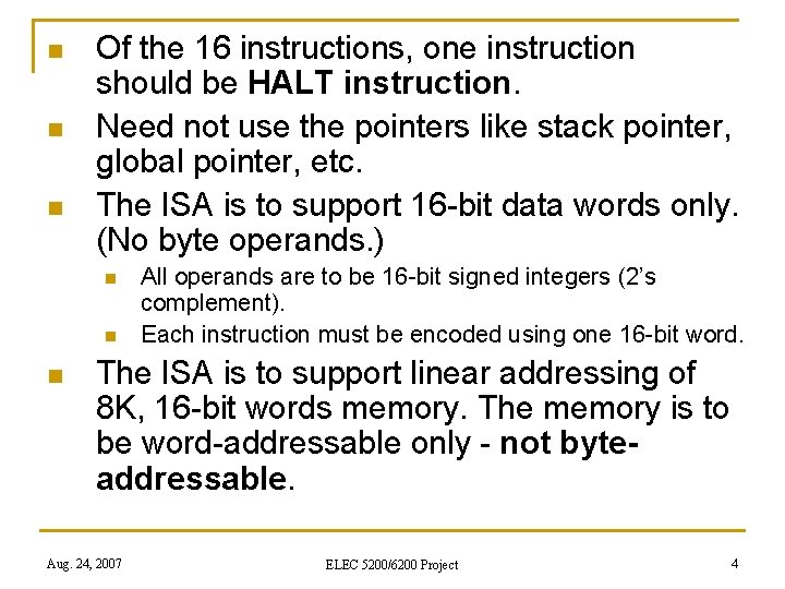
n n n Of the 16 instructions, one instruction should be HALT instruction. Need not use the pointers like stack pointer, global pointer, etc. The ISA is to support 16 -bit data words only. (No byte operands. ) n n n All operands are to be 16 -bit signed integers (2’s complement). Each instruction must be encoded using one 16 -bit word. The ISA is to support linear addressing of 8 K, 16 -bit words memory. The memory is to be word-addressable only - not byteaddressable. Aug. 24, 2007 ELEC 5200/6200 Project 4

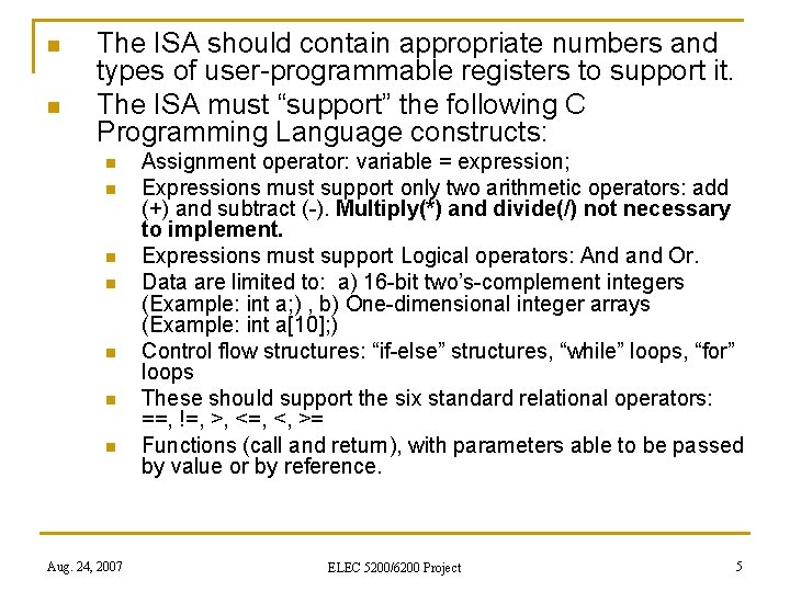
n n The ISA should contain appropriate numbers and types of user-programmable registers to support it. The ISA must “support” the following C Programming Language constructs: n n n n Aug. 24, 2007 Assignment operator: variable = expression; Expressions must support only two arithmetic operators: add (+) and subtract (-). Multiply(*) and divide(/) not necessary to implement. Expressions must support Logical operators: And and Or. Data are limited to: a) 16 -bit two’s-complement integers (Example: int a; ) , b) One-dimensional integer arrays (Example: int a[10]; ) Control flow structures: “if-else” structures, “while” loops, “for” loops These should support the six standard relational operators: ==, !=, >, <=, <, >= Functions (call and return), with parameters able to be passed by value or by reference. ELEC 5200/6200 Project 5

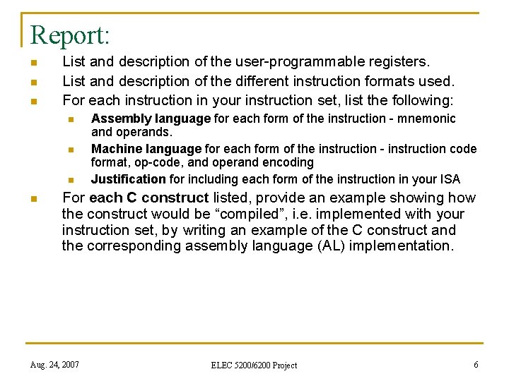
Report: n n n List and description of the user-programmable registers. List and description of the different instruction formats used. For each instruction in your instruction set, list the following: n n Assembly language for each form of the instruction - mnemonic and operands. Machine language for each form of the instruction - instruction code format, op-code, and operand encoding Justification for including each form of the instruction in your ISA For each C construct listed, provide an example showing how the construct would be “compiled”, i. e. implemented with your instruction set, by writing an example of the C construct and the corresponding assembly language (AL) implementation. Aug. 24, 2007 ELEC 5200/6200 Project 6

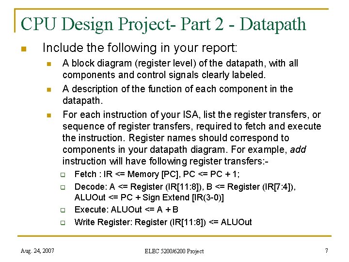
CPU Design Project- Part 2 - Datapath n Include the following in your report: n n n A block diagram (register level) of the datapath, with all components and control signals clearly labeled. A description of the function of each component in the datapath. For each instruction of your ISA, list the register transfers, or sequence of register transfers, required to fetch and execute the instruction. Register names should correspond to components in your datapath diagram. For example, add instruction will have following register transfers: q q Aug. 24, 2007 Fetch : IR <= Memory [PC], PC <= PC + 1; Decode: A <= Register (IR[11: 8]), B <= Register (IR[7: 4]), ALUOut <= PC + Sign Extend [IR(3 -0)] Execute: ALUOut <= A + B Write Register: Register (IR[11: 8]) <= ALUOut ELEC 5200/6200 Project 7

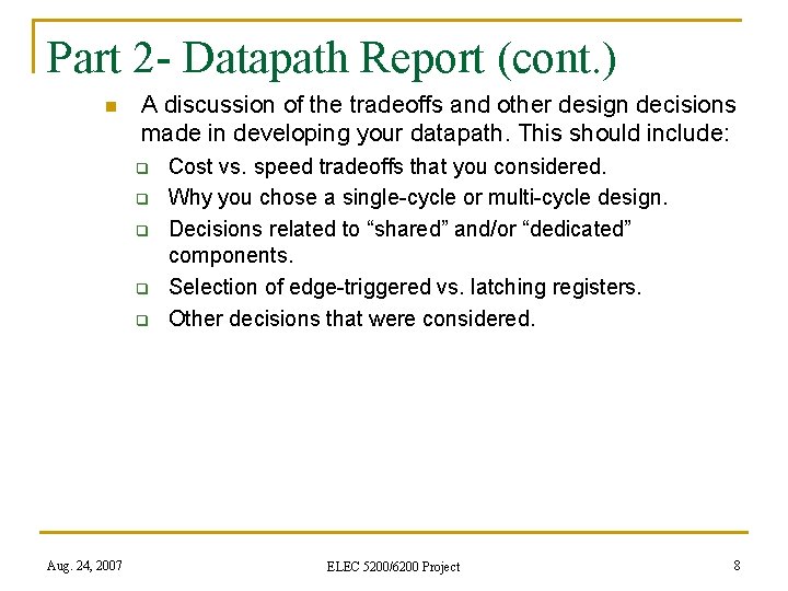
Part 2 - Datapath Report (cont. ) n A discussion of the tradeoffs and other design decisions made in developing your datapath. This should include: q q q Aug. 24, 2007 Cost vs. speed tradeoffs that you considered. Why you chose a single-cycle or multi-cycle design. Decisions related to “shared” and/or “dedicated” components. Selection of edge-triggered vs. latching registers. Other decisions that were considered. ELEC 5200/6200 Project 8

CPU Design Project- Part 3 - Datapath Verification n n Develop and verify a VHDL model of the datapath of your CPU, as described in the block diagram and register transfers defined in Part 2. The CPU must be capable of working with a single memory outside the CPU; the memory for Logic Simulation in Model. Sim will be added in Part 4, which will be the RAM block in the Altera Megafunctions Library. This is to be a register-transfer-level (RTL) design (not gate level). The datapath must have following external and internal ports: q q External ports: 16 -bit bidirectional databus and address bus, various control and status signals, 16 -bit port named “outvalue” which is used to display the contents of the particular register of the 16 registers in the final part of the project, Internal port: 4 -bit port named “inr” which is the register number of the particular register you want to select to display its content. Aug. 24, 2007 ELEC 5200/6200 Project 9

n n n Ports “outvalue” and “inr” along with clock and reset should be the only ports in your top-level of the design which will then be connected to the FPGA board. The datapath should be tested thoroughly by forcing the control inputs to selected values to mimic the operation of a control unit. Major Datapath Components likely to be needed: q ALU: The ALU must provide all arithmetic and logic functions required to support your instruction set. It should not provide unnecessary functions. q Register file: Design as a multi-port “memory array”. DO NOT instantiate individual registers ! q Sign/zero extension logic, as appropriate, for ALU inputs. q Program counter (PC). q Instruction register (IR) (if required). q Assorted multiplexers for data paths and register address inputs. Aug. 24, 2007 ELEC 5200/6200 Project 10

Report: n n Control Signal Table VHDL codes and List Format of the Simulations of each unique component used in the datapath VHDL code and List format of the Simulation of the top-level design of the datapath. Please annotate and explain your simulations. Aug. 24, 2007 ELEC 5200/6200 Project 11

CPU Design Project- Part 4 - Control Design and test a VHDL “behavioral” model of the control Unit n n n unit to realize the behavior described in your Control Signal Table from the previous part of the project. The test program will be provided to you. Hand compile the program into binary code and then use this code and modify the given RAM_init. mif file according to your program code. Using this. mif file create a 16 bit memory module from Altera’s Megafunction Library as explained in Mega. Wizard Plug-In Manager Manual. A. vhd file will be created in your working directory. Include this memory. vhd file in your datapath. Create a CPU component by instantiating and connecting your control unit and datapath components. CPU I/O ports should be limited to a clock, reset, inr as the input ports and outvalue as the output port. Aug. 24, 2007 ELEC 5200/6200 Project 12

Report: n n n VHDL code and simulation results of the Control Unit. Your assembly language code and binary code of the test program given to you. Final simulation of the test program of the top-level design. Show a sufficient set of control signals to demonstrate correct operation of each instruction (control unit state, address bus, data bus, ALU output, register file outputs, register file input, memory control signals, etc. ) On the simulation listing, annotate by writing the corresponding assembly language instruction next to each execute cycle and highlighting the “significant” result register or bus value. Aug. 24, 2007 ELEC 5200/6200 Project 13

CPU Design Project- Part 5 - Hardware (FPGA) Implementation and Demo n n Follow the Quartus II and DE 2 Manuals given to you for designing and implementing your circuit on the FPGA. Clock may be connected to any of the two freerunning clock frequencies available on the board, 27 MHz and 50 MHz. But for debugging your design using the manual clock by connecting it to one of 4 keys on the board will be an advantage and will make debugging easier. Run the program given to you and verify the results with your simulation in Part 4. You will demonstrate a working implementation of your design on a DE 2 Board. Aug. 24, 2007 ELEC 5200/6200 Project 14

Part 5 Report n Write a final report (no longer than one page) on: A. What you learned from the project. B. What would you do differently next time. C. Your advice to others doing such a project. Aug. 24, 2007 ELEC 5200/6200 Project 15