Chapter 19 MODERN FET STRUCTURES Sung June Kim



- Slides: 17

Chapter 19. MODERN FET STRUCTURES Sung June Kim kimsj@snu. ac. kr http: //nanobio. snu. ac. kr MODERN FET STRUCTURES

CONTENTS · Small-Dimension Effects · Select Structure Survey MODERN FET STRUCTURES

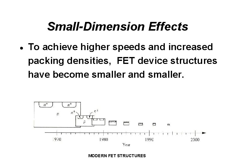
Small-Dimension Effects · To achieve higher speeds and increased packing densities, FET device structures have become smaller and smaller. MODERN FET STRUCTURES

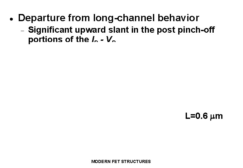
· Departure from long-channel behavior - Significant upward slant in the post pinch-off portions of the ID - VD L=0. 6 mm MODERN FET STRUCTURES

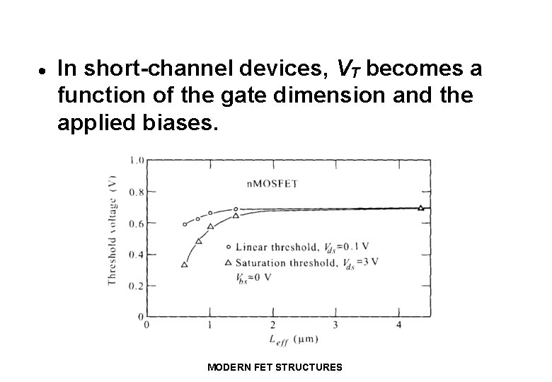
· In short-channel devices, VT becomes a function of the gate dimension and the applied biases. MODERN FET STRUCTURES

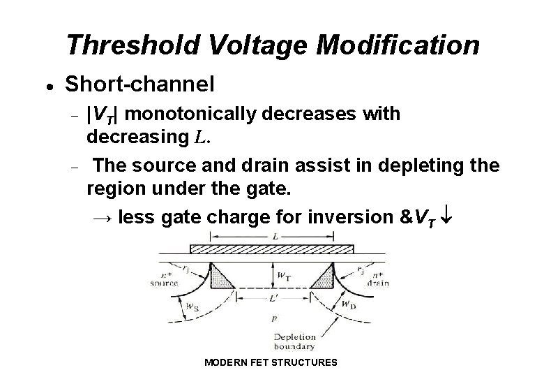
Threshold Voltage Modification · Short-channel - |VT| monotonically decreases with decreasing L. The source and drain assist in depleting the region under the gate. → less gate charge for inversion &VT MODERN FET STRUCTURES

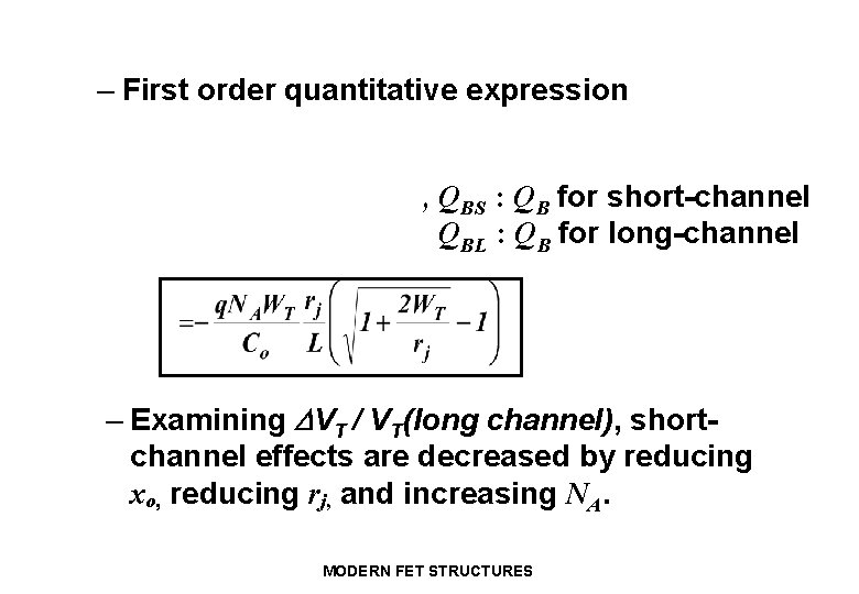
– First order quantitative expression , QBS : QB for short-channel QBL : QB for long-channel – Examining VT / VT(long channel), shortchannel effects are decreased by reducing xo, reducing rj, and increasing NA. MODERN FET STRUCTURES

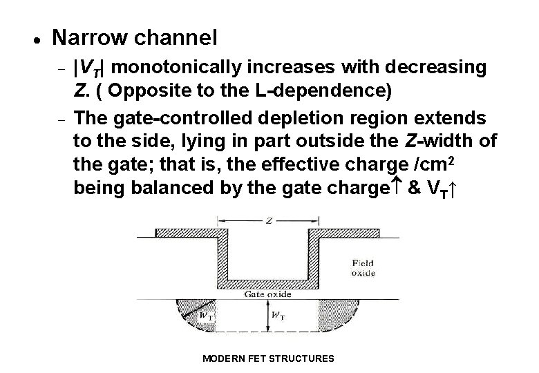
· Narrow channel - |VT| monotonically increases with decreasing Z. ( Opposite to the L-dependence) The gate-controlled depletion region extends to the side, lying in part outside the Z-width of the gate; that is, the effective charge /cm 2 being balanced by the gate charge & VT↑ MODERN FET STRUCTURES

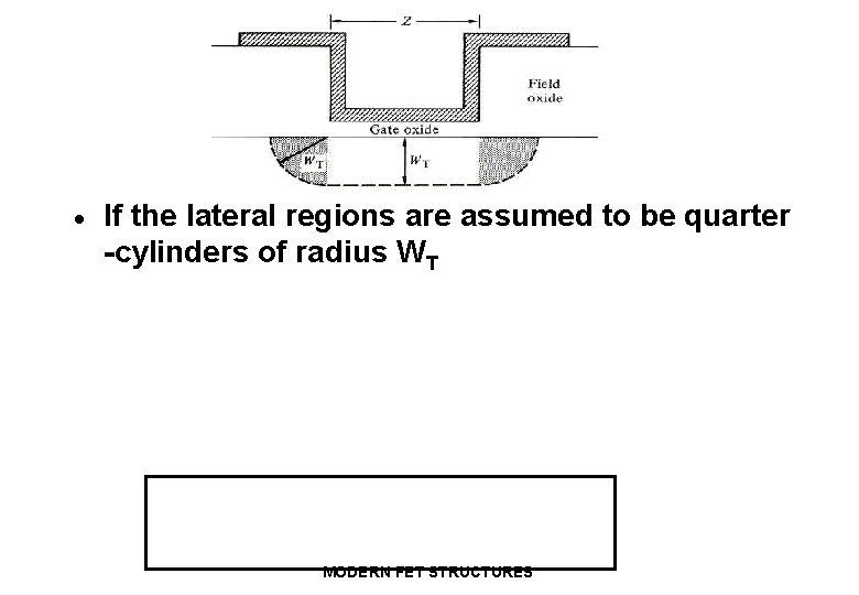
· If the lateral regions are assumed to be quarter -cylinders of radius WT MODERN FET STRUCTURES

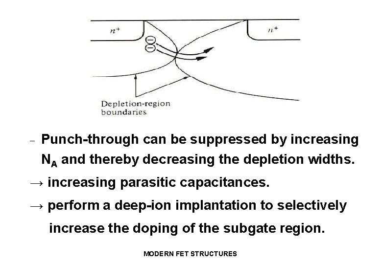
Parasitic BJT Action · · MOSFET bears a physical resemblance to a lateral BJT Punch-through - The depletion regions around the source and drain touch. The gate loses control of the subgate region and the ID flows beneath the surface through the touching depletion regions. MODERN FET STRUCTURES

- Punch-through can be suppressed by increasing NA and thereby decreasing the depletion widths. → increasing parasitic capacitances. → perform a deep-ion implantation to selectively increase the doping of the subgate region. MODERN FET STRUCTURES

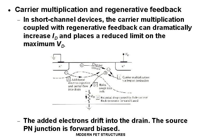
· Carrier multiplication and regenerative feedback - In short-channel devices, the carrier multiplication coupled with regenerative feedback can dramatically increase ID and places a reduced limit on the maximum VD. - The added electrons drift into the drain. The source PN junction is forward biased. MODERN FET STRUCTURES

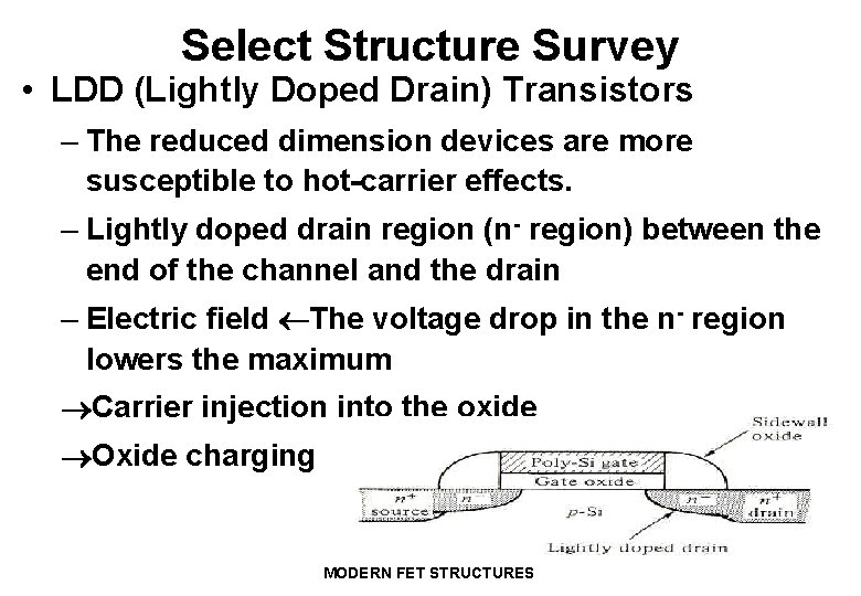
Hot-Carrier Effects · Oxide charging ( charge injection and trapping in the oxide ) - In the vicinity of the drain, some of carriers gain a sufficient amount of energy to surmount the Si. O 2 barrier. A charge build-up within the oxide A larger percentage of the gated region is affected in the smaller devices. Significant changes in VT and gm. - Oxide charging limits the useful “life” of a device. - To minimize hot-carrier effects, the LDD ( Lightly Doped Drain ) structure is used. - - MODERN FET STRUCTURES

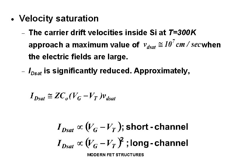
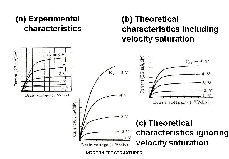
· Velocity saturation - The carrier drift velocities inside Si at T=300 K approach a maximum value of the electric fields are large. - IDsat is significantly reduced. Approximately, MODERN FET STRUCTURES when

(a) Experimental characteristics (b) Theoretical characteristics including velocity saturation (c) Theoretical characteristics ignoring velocity saturation MODERN FET STRUCTURES

· Ballistic Transport - If very small dimension structures have L< l ( the average distance between scattering events ), a large percentage of the carriers travel from the source to the drain without experiencing a single scattering event. - It can lead to super-fast devices. MODERN FET STRUCTURES

Select Structure Survey • LDD (Lightly Doped Drain) Transistors – The reduced dimension devices are more susceptible to hot-carrier effects. – Lightly doped drain region (n- region) between the end of the channel and the drain – Electric field The voltage drop in the n- region lowers the maximum Carrier injection into the oxide Oxide charging MODERN FET STRUCTURES