ASIC Technology Support and Foundry Services at CERN
- Slides: 20
ASIC Technology Support and Foundry Services at CERN Kostas Kloukinas CERN, PH-ESE dept. CH 1211, Geneve 23 Switzerland
ASIC Technology Support 14/2/13
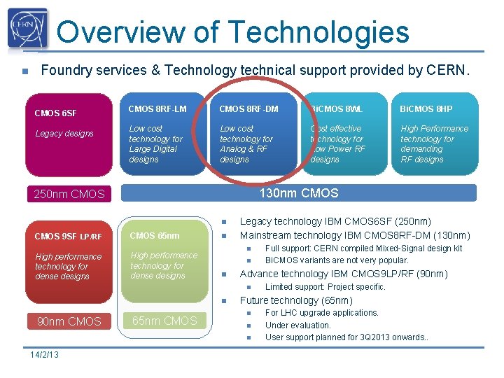
Overview of Technologies n Foundry services & Technology technical support provided by CERN. CMOS 6 SF Legacy designs CMOS 8 RF-LM CMOS 8 RF-DM Bi. CMOS 8 WL Bi. CMOS 8 HP Low cost technology for Large Digital designs Low cost technology for Analog & RF designs Cost effective technology for Low Power RF designs High Performance technology for demanding RF designs 130 nm CMOS 250 nm CMOS n CMOS 9 SF LP/RF CMOS 65 nm High performance technology for dense designs n Legacy technology IBM CMOS 6 SF (250 nm) Mainstream technology IBM CMOS 8 RF-DM (130 nm) n n n Advance technology IBM CMOS 9 LP/RF (90 nm) n n 90 nm CMOS 65 nm CMOS Limited support: Project specific. Future technology (65 nm) n n n 14/2/13 Full support: CERN compiled Mixed-Signal design kit Bi. CMOS variants are not very popular. For LHC upgrade applications. Under evaluation. User support planned for 3 Q 2013 onwards. .
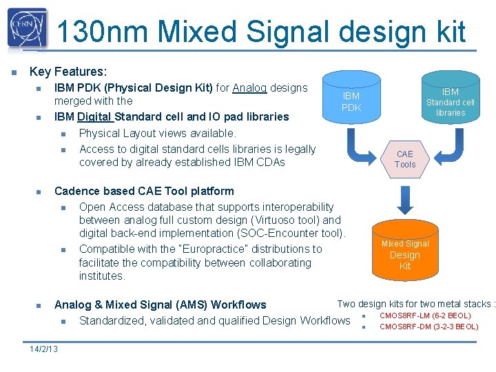
130 nm Mixed Signal design kit n Key Features: n n IBM PDK (Physical Design Kit) for Analog designs merged with the IBM Digital Standard cell and IO pad libraries n Physical Layout views available. n Access to digital standard cells libraries is legally covered by already established IBM CDAs IBM PDK Cadence based CAE Tool platform n Open Access database that supports interoperability between analog full custom design (Virtuoso tool) and digital back-end implementation (SOC-Encounter tool). n Compatible with the “Europractice” distributions to facilitate the compatibility between collaborating institutes. Standard cell libraries CAE Tools Mixed Signal Design Kit Two design kits for two metal stacks : Analog & Mixed Signal (AMS) Workflows n CMOS 8 RF-LM (6 -2 BEOL) n Standardized, validated and qualified Design Workflows n CMOS 8 RF-DM (3 -2 -3 BEOL) 14/2/13
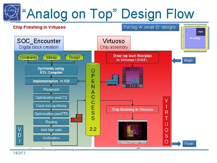
“Analog on Top” Design Flow Chip Finishing in Virtuoso For big ‘A’ small ‘D’ designs. SOC_Encounter Virtuoso Digital block creation Chip assembly Begin Finish 14/2/13
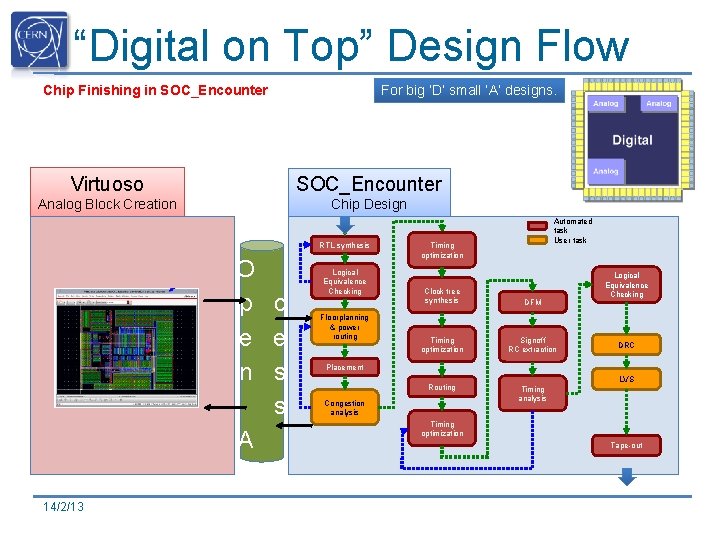
“Digital on Top” Design Flow Chip Finishing in SOC_Encounter For big ‘D’ small ‘A’ designs. Virtuoso SOC_Encounter Analog Block Creation Chip Design RTL synthesis O p c e e n s s A c 14/2/13 Logical Equivalence Checking Floorplanning & power routing Automated task User task Timing optimization Clock tree synthesis DFM Timing optimization Signoff RC extraction Routing Timing analysis Logical Equivalence Checking DRC Placement Congestion analysis LVS Timing optimization Tape-out
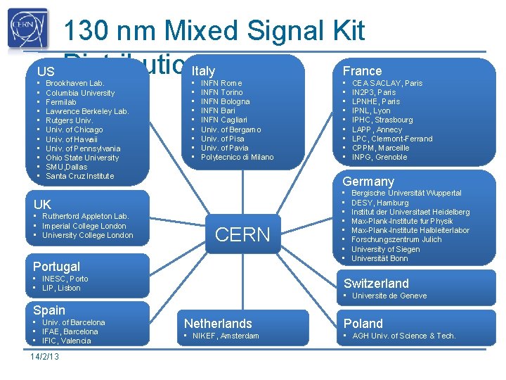
130 nm Mixed Signal Kit France Italy US Distribution • • • Brookhaven Lab. Columbia University Fermilab Lawrence Berkeley Lab. Rutgers Univ. of Chicago Univ. of Hawaii Univ. of Pennsylvania Ohio State University SMU, Dallas Santa Cruz Institute • • • INFN Rome INFN Torino INFN Bologna INFN Bari INFN Cagliari Univ. of Bergamo Univ. of Pisa Univ. of Pavia Polytecnico di Milano CERN Portugal • INESC, Porto • LIP, Lisbon Spain • Univ. of Barcelona • IFAE, Barcelona • IFIC, Valencia 14/2/13 CEA SACLAY, Paris IN 2 P 3, Paris LPNHE, Paris IPNL, Lyon IPHC, Strasbourg LAPP, Annecy LPC, Clermont-Ferrand CPPM, Marceille INPG, Grenoble Germany UK • Rutherford Appleton Lab. • Imperial College London • University College London • • • • • Bergische Universität Wuppertal DESY, Hamburg Institut der Universitaet Heidelberg Max-Plank-Institute fur Physik Max-Plank-Institute Halbleiterlabor Forschungszentrum Julich University of Siegen Universität Bonn Switzerland • Universite de Geneve Netherlands Poland • NIKEF, Amsterdam • AGH Univ. of Science & Tech.
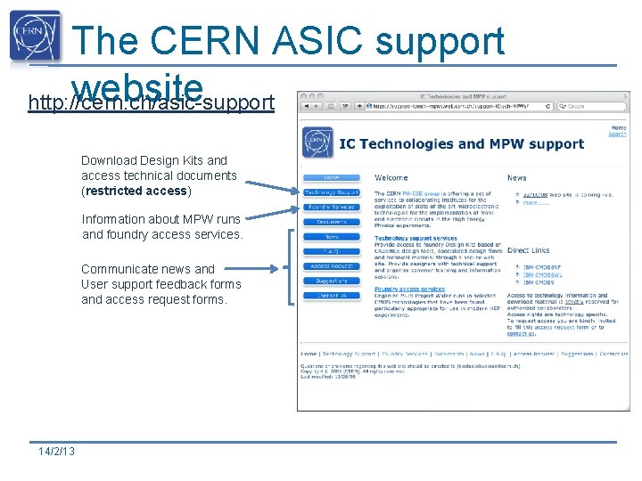
The CERN ASIC support website http: //cern. ch/asic-support Download Design Kits and access technical documents (restricted access) Information about MPW runs and foundry access services. Communicate news and User support feedback forms and access request forms. 14/2/13
Foundry Access Services 14/2/13
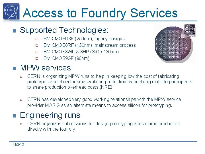
Access to Foundry Services n Supported Technologies: q q n MPW services: q q n IBM CMOS 6 SF (250 nm), legacy designs IBM CMOS 8 RF (130 nm), mainstream process IBM CMOS 8 WL & 8 HP (Si. Ge 130 nm) IBM CMOS 9 SF (90 nm) CERN is organizing MPW runs to help in keeping low the cost of fabricating prototypes and allow for small-volume production by enabling multiple participants to share production overhead costs (NRE). CERN has developed very good working relationships with the MPW service provider MOSIS as an alternate means to access silicon for prototyping. Engineering runs q 14/2/13 CERN organizes submissions for design prototyping and volume production directly with the foundry.
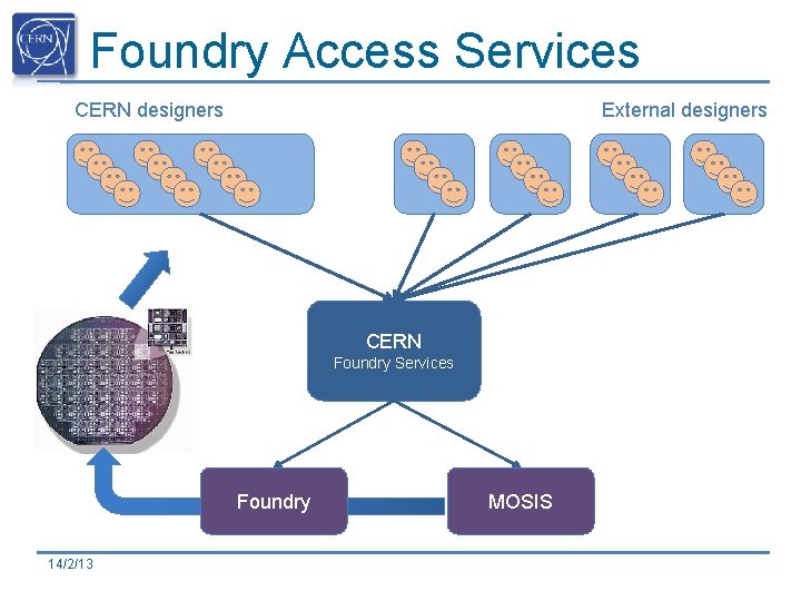
Foundry Access Services CERN designers External designers CERN Foundry Services Foundry 14/2/13 MOSIS
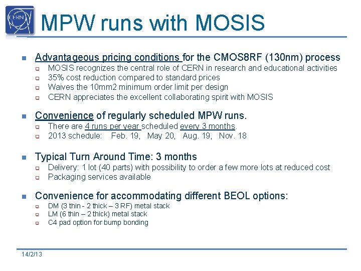
MPW runs with MOSIS n Advantageous pricing conditions for the CMOS 8 RF (130 nm) process q q n Convenience of regularly scheduled MPW runs. q q n There are 4 runs per year scheduled every 3 months. 2013 schedule: Feb. 19, May 20, Aug. 19, Nov. 18 Typical Turn Around Time: 3 months q q n MOSIS recognizes the central role of CERN in research and educational activities 35% cost reduction compared to standard prices Waives the 10 mm 2 minimum order limit per design CERN appreciates the excellent collaborating spirit with MOSIS Delivery: 1 lot (40 parts) with possibility to order a few more lots at reduced cost Packaging services available Convenience for accommodating different BEOL options: q q q 14/2/13 DM (3 thin - 2 thick – 3 RF) metal stack LM (6 thin – 2 thick) metal stack C 4 pad option for bump bonding
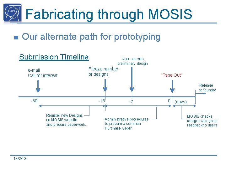
Fabricating through MOSIS n Our alternate path for prototyping Submission Timeline e-mail Call for interest User submits preliminary design Freeze number of designs “Tape Out” Release to foundry -30 -15 Register new Designs on MOSIS website and prepare paperwork. 14/2/13 -7 Administrative procedures to prepare a common Purchase Order. 0 (days) MOSIS checks designs and gives feedback to users
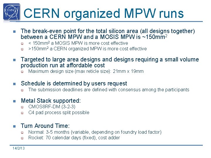
CERN organized MPW runs n The break-even point for the total silicon area (all designs together) between a CERN MPW and a MOSIS MPW is ~150 mm 2 q q n Targeted to large area designs and designs requiring a small volume production run at affordable cost q n The submission deadlines are defined with consensus among the participants Metal Stack supported: q q n Maximum design size (max reticle size): 21 mm x 19 mm Schedule is determined by users request q n < 150 mm 2 a MOSIS MPW is more cost effective >150 mm 2 a CERN organized MPW is more cost effective CMOS 8 RF-DM (3 -2 -3) C 4 pad process split possible Turn Around Time: q q 14/2/13 Normal: 3 -5 months (variable, depending on foundry load factor) Rocket: 70 calendar days (fixed), cost adder
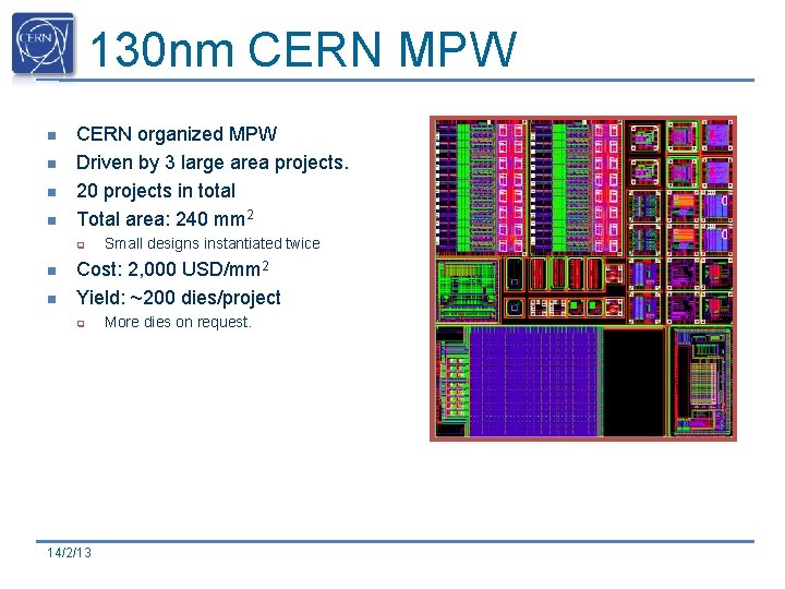
130 nm CERN MPW n n CERN organized MPW Driven by 3 large area projects. 20 projects in total Total area: 240 mm 2 q n n Small designs instantiated twice Cost: 2, 000 USD/mm 2 Yield: ~200 dies/project q 14/2/13 More dies on request.
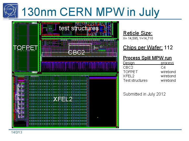
130 nm CERN MPW in July 2012 test structures Reticle Size: X= 14, 595, Y=14, 710 TOFPET CBC 2 Chips per Wafer: 112 Process Split MPW run Design CBC 2 TOFPET XFEL 2 Test structures XFEL 2 14/2/13 process C 4 wirebond Submitted in July 2012
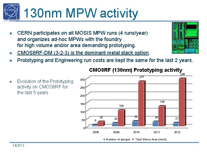
130 nm MPW activity n n n CERN participates on all MOSIS MPW runs (4 runs/year) and organizes ad-hoc MPWs with the foundry for high volume and/or area demanding prototyping. CMOS 8 RF-DM (3 -2 -3) is the dominant metal stack option. Prototyping and Engineering run costs are kept the same for the last 2 years. CMO 8 RF (130 nm) Prototyping activity n Evolution of the Prototyping activity on CMOS 8 RF for the last 5 years 295 277 300 250 200 125 150 100 50 8 28 20 32 28 21 2010 2011 2012 0 2008 2009 Number of designs 14/2/13 Total Silicon Area (mm 2)
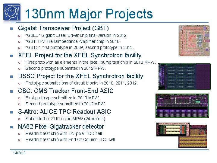
130 nm Major Projects n Gigabit Transceiver Project (GBT) q q q n XFEL Project for the XFEL Synchrotron facility q q n q First prototype submitted in 2010 MPW. Second prototype submitted in 2012 MPW. S-Altro: ALICE TPC Readout ASIC q n Prototype submissions of circuit blocks in 2010, 2011, 2012. CBC: CMS Tracker Front-End ASIC q n First proto with all elements in the pixel, bump test chip in 2010 MPW. Second prototype submitted in 2012 MPW. DSSC Project for the XFEL Synchrotron facility q n “GBLD” Gigabit Laser Driver chip final version in 2012. “GBT-TIA” Transimpedance Amplifier chip in 2010. “GBTX”, first prototype in 2009, second prototype in 2012. Submitted in 2010 on an MPW (24 wafers). NA 62 Pixel Gigatracker detector q q 14/2/13 Readout test chip with ON pixel TDC cell Readout test chip with End-Of-Column TDC cell
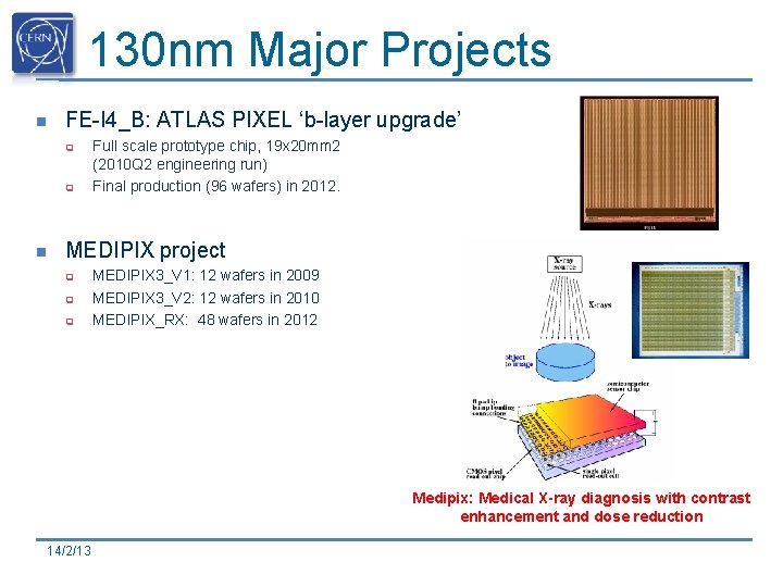
130 nm Major Projects n FE-I 4_B: ATLAS PIXEL ‘b-layer upgrade’ q q n Full scale prototype chip, 19 x 20 mm 2 (2010 Q 2 engineering run) Final production (96 wafers) in 2012. MEDIPIX project q q q MEDIPIX 3_V 1: 12 wafers in 2009 MEDIPIX 3_V 2: 12 wafers in 2010 MEDIPIX_RX: 48 wafers in 2012 Medipix: Medical X-ray diagnosis with contrast enhancement and dose reduction 14/2/13
Thank You 14/2/13