2003 Indium Phosphide and Related Materials May 13
- Slides: 16

2003 Indium Phosphide and Related Materials, May 13, Santa Barbara 200 GHz fmax, ft In. P/In 0. 53 Ga 0. 47 As/In. P Metamorphic Double Heterojunction Bipolar Transistors on Ga. As Substrates Y. M. Kim, M. Urteaga, M. Dahlström, M. J. W. Rodwell, A. C. Gossard Department of Electrical Engineering, Materials Department, University of California, Santa Barbara kymdow@ece. ucsb. edu 805 -893 -3543, 413 -208 -9864 fax

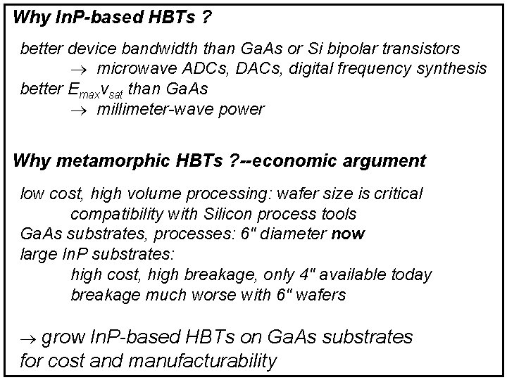
Why In. P-based HBTs ? better device bandwidth than Ga. As or Si bipolar transistors ® microwave ADCs, DACs, digital frequency synthesis better Emaxvsat than Ga. As ® millimeter-wave power Why metamorphic HBTs ? --economic argument low cost, high volume processing: wafer size is critical compatibility with Silicon process tools Ga. As substrates, processes: 6" diameter now large In. P substrates: high cost, high breakage, only 4" available today breakage much worse with 6" wafers ® grow In. P-based HBTs on Ga. As substrates for cost and manufacturability

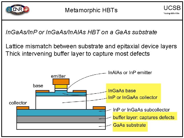
Metamorphic HBTs UCSB Young-Min Kim In. Ga. As/In. P or In. Ga. As/In. Al. As HBT on a Ga. As substrate Lattice mismatch between substrate and epitaxial device layers Thick intervening buffer layer to capture most defects

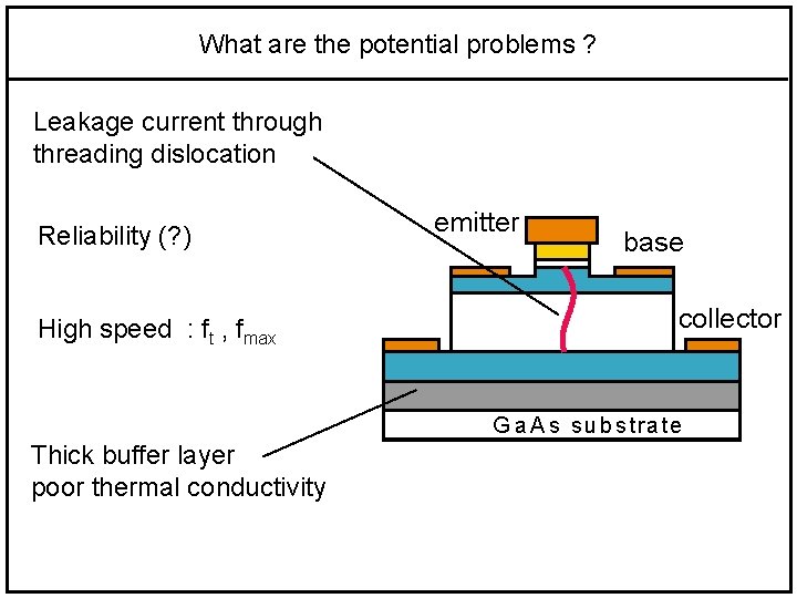
What are the potential problems ? Leakage current through threading dislocation Reliability (? ) High speed : ft , fmax emitter base collector G a A s s u b s tra te Thick buffer layer poor thermal conductivity

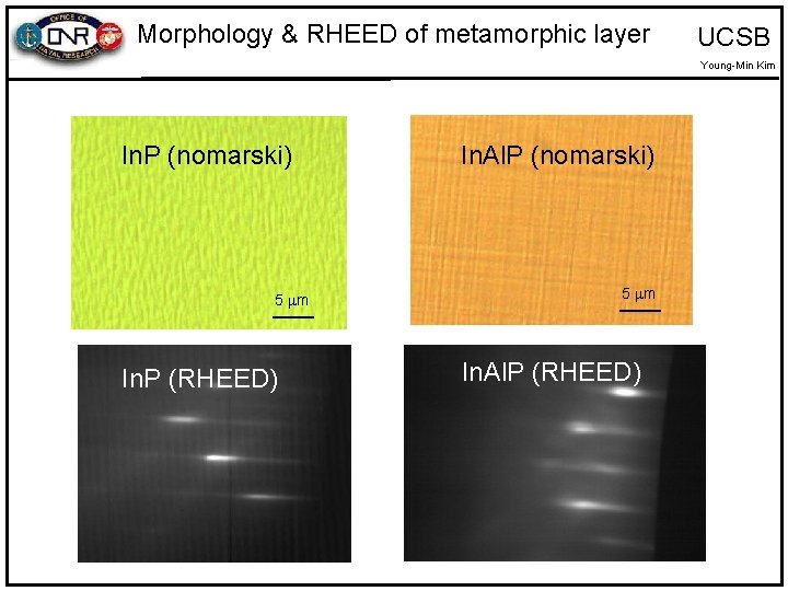
Morphology & RHEED of metamorphic layer UCSB Young-Min Kim Al. Ga. As. Sb In. P (nomarski) 5 m In. P (RHEED) In. Al. As In. Al. P (nomarski) 5 m In. Al. P (RHEED)

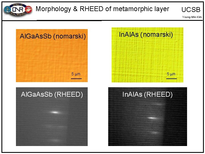
Morphology & RHEED of metamorphic layer UCSB Young-Min Kim Al. Ga. As. Sb (nomarski) 5 m Al. Ga. As. Sb (RHEED) In. Al. As (nomarski) 5 m In. Al. As (RHEED)

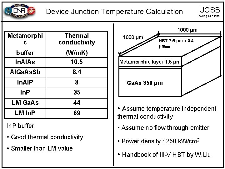
Device Junction Temperature Calculation Metamorphi c Thermal conductivity buffer In. Al. As (W/m. K) 10. 5 Al. Ga. As. Sb 8. 4 In. Al. P 8 In. P 35 LM Ga. As 44 LM In. P 69 In. P buffer • Good thermal conductivity • Smaller than LM value UCSB Young-Min Kim 1000 μm HBT 7. 5 μm x 0. 4 μm Metamorphic layer 1. 5 μm Ga. As 350 μm • Assume temperature independent thermal conductivity • Assume no flow through emitter • Power density : 250 k. W/cm 2 • Handbook of III-V HBT by W. Liu

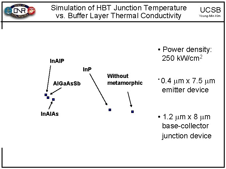
Simulation of HBT Junction Temperature vs. Buffer Layer Thermal Conductivity UCSB Young-Min Kim • Power density: 250 k. W/cm 2 In. Al. P In. P Al. Ga. As. Sb In. Al. As Without metamorphic m x 7. 5 m emitter device • 0. 4 • 1. 2 m x 8 m base-collector junction device

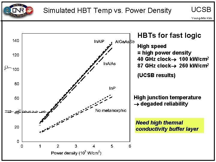
Simulated HBT Temp vs. Power Density UCSB Young-Min Kim HBTs for fast logic High speed = high power density 40 GHz clock® 100 k. W/cm 2 87 GHz clock® 260 k. W/cm 2 (UCSB results) High junction temperature ® degaded reliability Need high thermal conductivity buffer layer

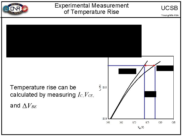
Experimental Measurement of Temperature Rise Temperature rise can be calculated by measuring and UCSB Young-Min Kim

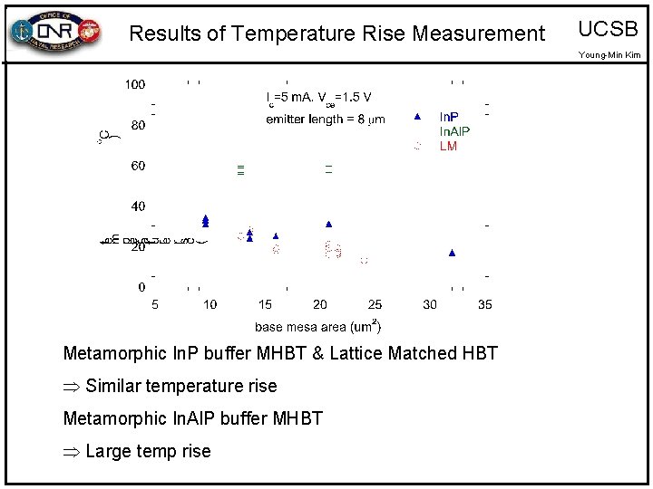
Results of Temperature Rise Measurement UCSB Young-Min Kim Metamorphic In. P buffer MHBT & Lattice Matched HBT Þ Similar temperature rise Metamorphic In. Al. P buffer MHBT Þ Large temp rise

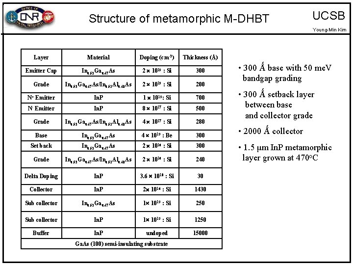
Structure of metamorphic M-DHBT UCSB Young-Min Kim Layer Material Doping (cm-3) Thickness (Å) Emitter Cap In 0. 53 Ga 0. 47 As 2 1019 : Si 300 Grade In 0. 53 Ga 0. 47 As/In 0. 52 Al 0. 48 As 2 1019 : Si 200 N+ Emitter In. P 1 1019: Si 700 N- Emitter In. P 8 1017 : Si 500 Grade In 0. 53 Ga 0. 47 As/In 0. 52 Al 0. 48 As 4 1017 : Si 280 Base In 0. 53 Ga 0. 47 As 4 1019 : Be 300 Set back In 0. 53 Ga 0. 47 As 2 1016 : Si 300 Grade In 0. 53 Ga 0. 47 As/In 0. 52 Al 0. 48 As 2 1016 : Si 240 Delta Doping In. P 3. 6 1018 : Si 30 Collector In. P 2 1016 : Si 1430 Sub collector In 0. 53 Ga 0. 47 As 1 1019 : Si 250 Sub collector In. P 1 1019 : Si 1250 Buffer In. P undoped 15000 Ga. As (100) semi-insulating substrate • 300 Ǻ base with 50 me. V bandgap grading • 300 Ǻ setback layer between base and collector grade • 2000 Ǻ collector • 1. 5 μm In. P metamorphic layer grown at 470 o. C

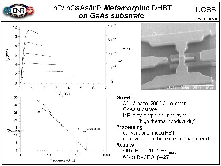
In. P/In. Ga. As/In. P Metamorphic DHBT on Ga. As substrate UCSB Young-Min Kim Growth: 300 Å base, 2000 Å collector Ga. As substrate In. P metamorphic buffer layer (high thermal conductivity) Processing conventional mesa HBT narrow 1. 2 um base mesa, 0. 4 um emitter Results 200 GHz ft, 200 GHz fmax, 6 Volt BVCEO, b=27

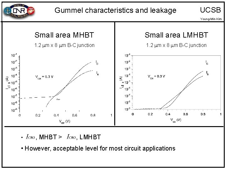
Gummel characteristics and leakage UCSB Young-Min Kim • Small area MHBT Small area LMHBT 1. 2 m x 8 m B-C junction , MHBT > , LMHBT • However, acceptable level for most circuit applications

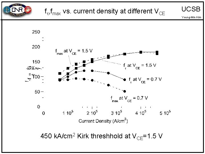
f , fmax vs. current density at different VCE 450 k. A/cm 2 Kirk threshhold at VCE=1. 5 V UCSB Young-Min Kim

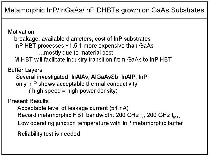
Metamorphic In. P/In. Ga. As/In. P DHBTs grown on Ga. As Substrates Motivation breakage, available diameters, cost of In. P substrates In. P HBT processes ~1. 5: 1 more expensive than Ga. As …mostly due to material cost M-HBT will facilitate industry transition from Ga. As to In. P HBT Buffer Layers Several investigated: In. Al. As, Al. Ga. As. Sb, In. Al. P, In. P only In. P shows acceptable thermal conductivity ( high speed = high power density) Present Results Acceptable level of leakage current (54 n. A) Record metamorphic HBT bandwidth: 200 GHz f , 200 GHz fmax Low operating junction temperature with In. P metamorphic buffer Reliability test is needed