n n Indium oxide doped with tin oxide

 is balanced against")


 and La 0. 7 Ca")


- Slides: 25
n n Indium oxide doped with tin oxide, ITO, is used to make transparent conductive coatings. Thin film layers can be deposited by electron-beam evaporation or sputtering. Typical applications of ITO-coated substrates include touch panel contacts, electrodes for LCD and electrochromic displays, energy conserving architectural windows, defogging aircraft and automobile windows, heat-reflecting coatings to increase light bulb efficiency, gas sensors, antistatic window coatings, wear resistant layers on glass, etc.
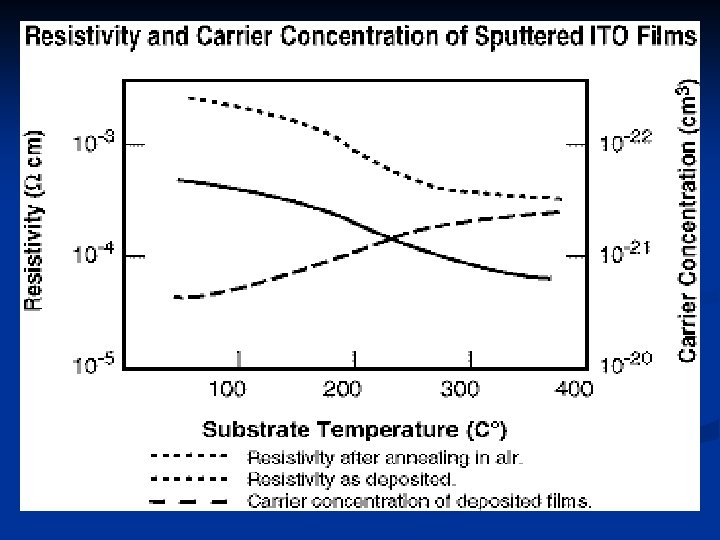
Film Properties n n n High conductivity (or low sheet resistance) is balanced against high transmission in the visible region. Sheet resistance can be less than 10 Ohms/sq. with a visible transmission of >80%. To obtain transmission near 90%, sheet resistance must be >100 Ohms/sq. ITO films behave as metals to long wavelength light because of the presence of a plasma wavelength above 1 µm. At longer wavelengths, the film becomes reflecting, and the IR reflectance is related to the sheet resistance of the film; sheet resistance must be <30 Ohms/sq. to obtain IR reflectance >80%.
Physical Properties of Solid ITO Material n n Molecular Weight Varies with composition Melting Point~1900° C Color Light yellow to gray, depending on degree of oxidation Crystal Density~7. 14 g/cc
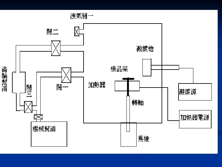
Schematic diagram of the rf sputtering system used in this work ITO YBa 2 Cu 3 Oy 3. 5 cm rf sputtering gun Ar+O 2 gas 5. 3 cm Nd 0. 7 Sr 0. 3 Mn. O 3 Pr. Ba 2 Cu 3 Oy 3 cm shutter sample holder water-cooled stainless-steel shielding L. M. Wang, H. W. Yu, H. C. Yang and H. E. Horng, Physica C, 256, 57 (1996).
n Sputtered Film Applications The high oxide composition of high density target and bulk ITO forms make them ideal for low temperature applications, such as polymer substrates for LCD, touch panels, and other high volume production needs.
OUTLINE n n Introduction Experiments Growth of superlattices Transport Properties Results and Discussion -2 X-diffraction pattern Hall coefficients Flux pinning Dimensinality Conclusion
In this work , we investigated the flux pinning, the mixed state Hall coefficients, the superconductivity and magnetoresistance of YBCO/RMMO multilayers. The results are compared with that of YBa 2 Cu 3 Oy/Pr. Ba 2 Cu 3 Oy (YBCO/PBCO) superlattices. YBCO/RMMO: YBCO/RMMO YBa 2 Cu 3 Oy/R 0. 7 M 0. 3 Mn. O 3 with R = La or Nd and M = Ca and Sr YBCO/PBCO : YBa 2 Cu 3 Oy/Pr. Ba 2 Cu 3 Oy R RMMO is ferromagnetic, whereas PBCO is insulating at low temperatures.
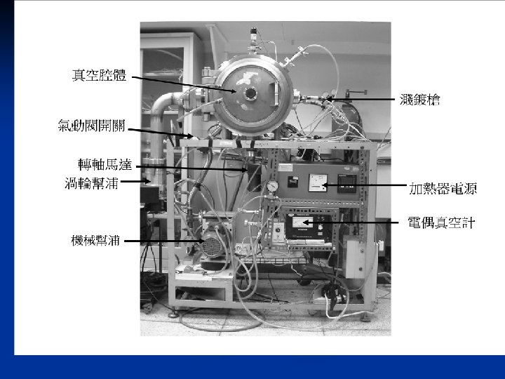
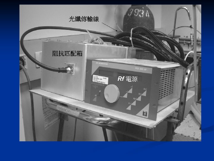
Sample preparation The superlattices were prepared by the rf magnetron sputtering method.
Crystal Structure of YBa 2 Cu 3 Oy (YBCO) and La 0. 7 Ca 0. 3 Mn. O 3 (LCMO): a (5. 47 Å) Mn O La, Ca c (7. 74 Å) b (5. 46 Å) YBa 2 Cu 3 Oy La 0. 7 Ca 0. 3 Mn. O 3
1 m Surface morphology of an as grown YBCO film with root mean square roughness of about 8. 2 Å
● AFM image La 0. 7 Ca 0. 3 Mn. Oy Scanned area = 30 m; RMS roughness = 8. 4 Å
● X-ray diffraction 2 d sinθ= λ θ d θ D 2 D sinθ= λ D = /2(sin n+1 - sin n) YBCO LCMO * * STO Satellite peak * * n n+1
n -2 X-diffraction pattern
-2 x-ray diffraction pattern of a (YBa 2 Cu 3 Oy/Pr. Ba 2 Cu 3 Oy) (96 Å/60 Å) 10 superlattice. 10
NSMO and LCMO films show the Curie temperature at 222 K and 250 K respectively.
n Transport Measurements in magnetic fields Resistivity Hall measurements
● The pattern for resistivity and Hall measurements V = V 3 -V 2→Resistance Vh = V 2 -V 1→Hall coefficient