Weekly Report Renjie Chen Supervisor Shadi A Dayeh
- Slides: 9
Weekly Report Renjie Chen Supervisor: Shadi A. Dayeh
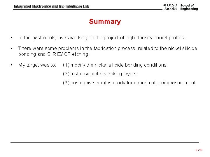
Integrated Electronics and Bio-interfaces Lab Summary • In the past week, I was working on the project of high-density neural probes. • There were some problems in the fabrication process, related to the nickel silicide bonding and Si RIE/ICP etching. • My target was to: (1) modify the nickel silicide bonding conditions (2) test new metal stacking layers (3) push new samples ready for neural culture/measurement 2 /10
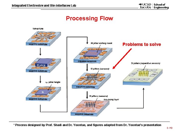
Integrated Electronics and Bio-interfaces Lab Processing Flow Problems to solve * Process designed by Prof. Shadi and Dr. Yoontae, and figures adapted from Dr. Yoontae’s presentation 3 /10
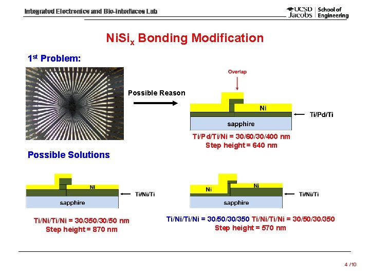
Integrated Electronics and Bio-interfaces Lab Ni. Six Bonding Modification 1 st Problem: Possible Reason Ti/Pd/Ti/Ni = 30/60/30/400 nm Step height = 640 nm Possible Solutions Ti/Ni/Ti/Ni = 30/350/30/50 nm Step height = 870 nm Ti/Ni/Ti/Ni = 30/50/30/350 Step height = 570 nm 4 /10
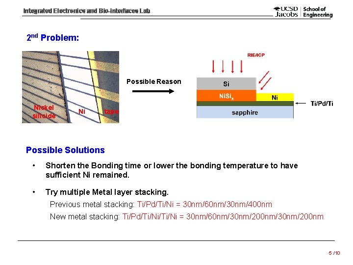
Integrated Electronics and Bio-interfaces Lab 2 nd Problem: Possible Reason Nickel silicide Ni tape Possible Solutions • Shorten the Bonding time or lower the bonding temperature to have sufficient Ni remained. • Try multiple Metal layer stacking. Previous metal stacking: Ti/Pd/Ti/Ni = 30 nm/60 nm/30 nm/400 nm New metal stacking: Ti/Pd/Ti/Ni = 30 nm/60 nm/30 nm/200 nm 5 /10
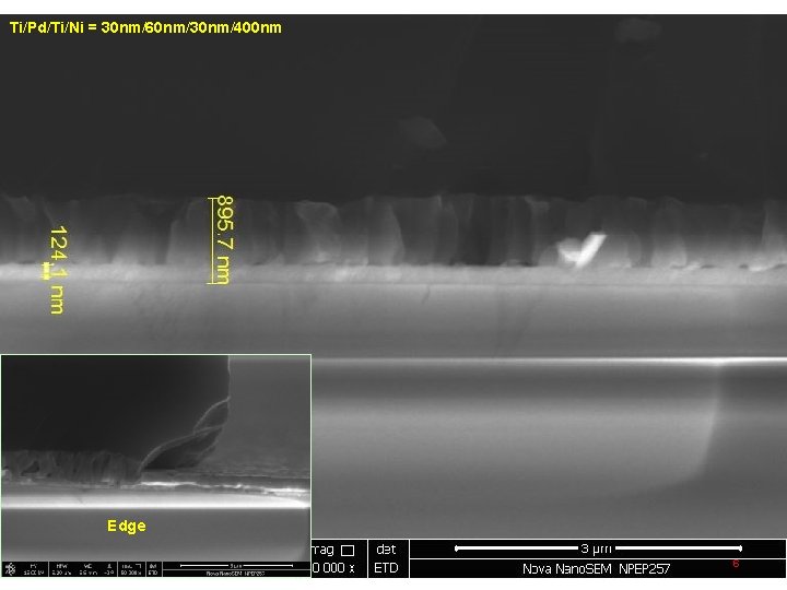
Integrated Electronics and Bio-interfaces Lab Ti/Pd/Ti/Ni = 30 nm/60 nm/30 nm/400 nm Edge 6 /10
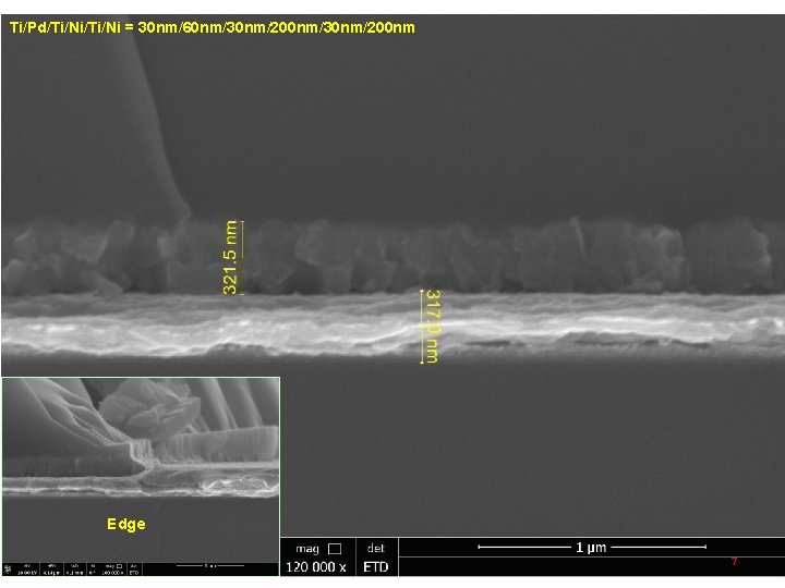
Integrated Electronics and Bio-interfaces Lab Ti/Pd/Ti/Ni = 30 nm/60 nm/30 nm/200 nm Edge 7 /10
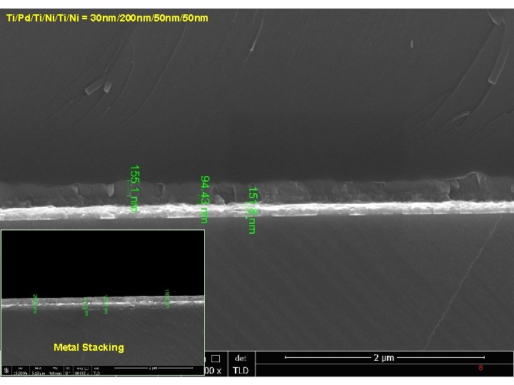
Integrated Electronics and Bio-interfaces Lab Ti/Pd/Ti/Ni = 30 nm/200 nm/50 nm Metal Stacking 8 /10
Integrated Electronics and Bio-interfaces Lab Plan 1. Samples send back to UCSD for thinning/pillar etching 7 Samples with old metal stacking (Ti/Pd/Ti/Ni) finished -- 5 samples bonded with 90 um Si, for Si thinning -> send back -- 2 samples bonded with 10 um Si, for pillar etching -> directly use for device 9 Samples with new metal stacking (Ti/Pd/Ti/Ni) in preparation -- 7 samples to be bonded with 90 um Si, for Si thinning -> send back -- 2 samples to be bonded with 10 um Si, for pillar etching -> directly use for device 2. During waiting for samples coming back -- work on Ni-In. Ga. As project -- Cory’s EBL sample, may take some time to calibrate the off-set -- Farid’s Photomask has finished, will be mailed together with my samples 9 /10