Weekly Group Meeting Report Renjie Chen Supervisor Prof
- Slides: 10

Weekly Group Meeting Report Renjie Chen Supervisor: Prof. Shadi A. Dayeh

Integrated Electronics and Bio-interfaces Lab Summary • In the past week, I was finishing the samples of high-density neural probes, and starting to work on Ni-In. Ga. As diffusion study. • My target was to: (1) prepare enough neural probe samples to send back to UCSD for Si etching (2) Modify the mask design for Ni-In. Ga. As Fin structures (3) Fabricate Ni-In. Ga. As Fin structures for temperature dependent diffusion study 2 /9

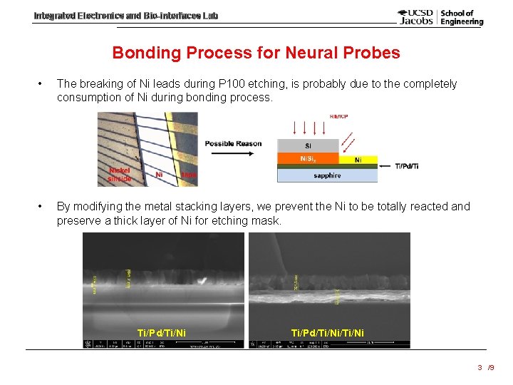
Integrated Electronics and Bio-interfaces Lab Bonding Process for Neural Probes • The breaking of Ni leads during P 100 etching, is probably due to the completely consumption of Ni during bonding process. • By modifying the metal stacking layers, we prevent the Ni to be totally reacted and preserve a thick layer of Ni for etching mask. Ti/Pd/Ti/Ni/Ti/Ni 3 /9

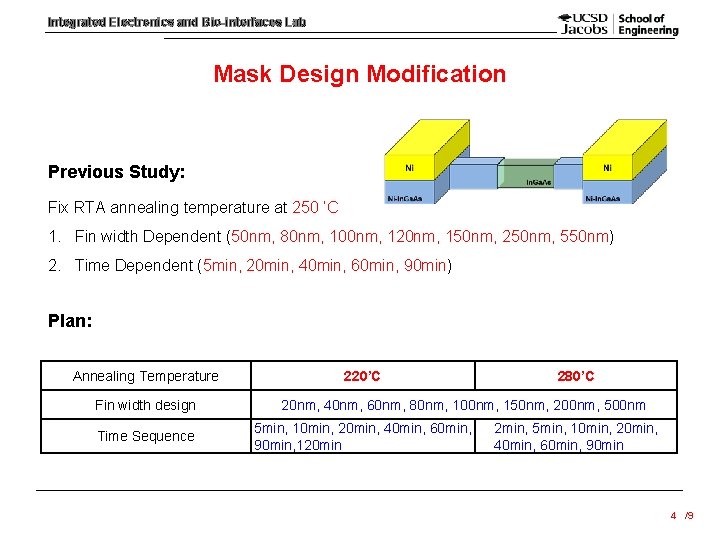
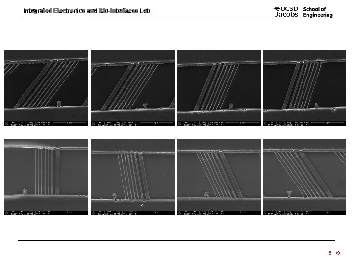
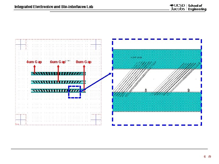
Integrated Electronics and Bio-interfaces Lab Mask Design Modification Previous Study: Fix RTA annealing temperature at 250 ‘C 1. Fin width Dependent (50 nm, 80 nm, 100 nm, 120 nm, 150 nm, 250 nm, 550 nm) 2. Time Dependent (5 min, 20 min, 40 min, 60 min, 90 min) Plan: Annealing Temperature Fin width design Time Sequence 220’C 280’C 20 nm, 40 nm, 60 nm, 80 nm, 100 nm, 150 nm, 200 nm, 500 nm 5 min, 10 min, 20 min, 40 min, 60 min, 90 min, 120 min 2 min, 5 min, 10 min, 20 min, 40 min, 60 min, 90 min 4 /9

Integrated Electronics and Bio-interfaces Lab 5 /9

Integrated Electronics and Bio-interfaces Lab 4 um Gap 6 um Gap 8 um Gap 6 /9

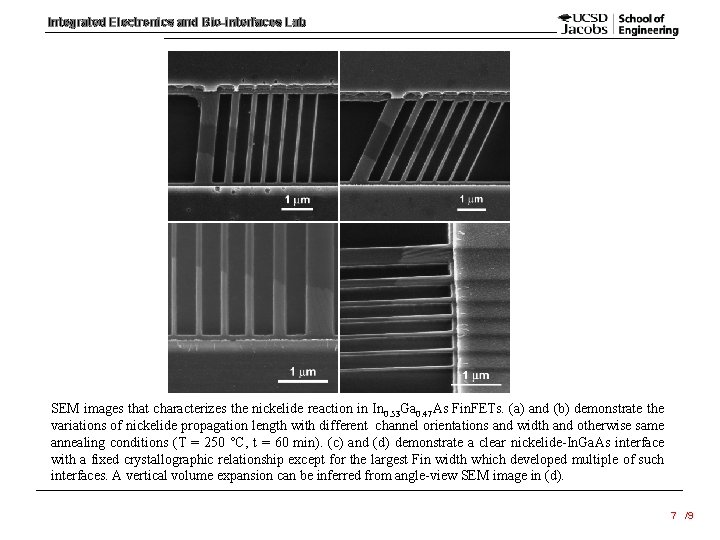
Integrated Electronics and Bio-interfaces Lab SEM images that characterizes the nickelide reaction in In 0. 53 Ga 0. 47 As Fin. FETs. (a) and (b) demonstrate the variations of nickelide propagation length with different channel orientations and width and otherwise same annealing conditions (T = 250 °C, t = 60 min). (c) and (d) demonstrate a clear nickelide-In. Ga. As interface with a fixed crystallographic relationship except for the largest Fin width which developed multiple of such interfaces. A vertical volume expansion can be inferred from angle-view SEM image in (d). 7 /9

Integrated Electronics and Bio-interfaces Lab Ni-In. Ga. As Fin Structure Fabrication • When I first arrived at CINT 3 weeks ago, I tried to transfer In. Ga. As layer onto Si twice and they were not successful. In one time, the In. Ga. As layer was separated from the Si wafer during HCl etching. In the other time, the In. Ga. As layer was also etching in the concentrated HCl solution. • Now the bonding problem was solved, and I realized that the In. P layer should be lapped down to below 100 um (tricky for lapping process) in order to shorten the time that the samples are later on immersed in the HCl solution. At the same time, 3: 1 HCl in DI should be used for elective etching of In. P, because concentrated HCl will also dissolve In. Ga. As layer. • Now 12 samples on two large chips have been processed, and the 2 nd EBL step for Ni lines deposition has finished. The Fin writing will be processed tonight. 8 /9

Integrated Electronics and Bio-interfaces Lab Plan 1. Continue to finish the fabrication of Ni-In. Ga. As fin structures on Si wafer. -- EBL writing for Fin layer, followed by In. Ga. As dry etching and surface smoothing -- RTA will be perform at two temperature and different time interval for these 12 samples -- AFM will be used to measure the surface profile of the reacted Ni-In. Ga. As -- Measure & plot the nickelide length with different fin width and reaction time 2. Wait for feedback from P 100 etching on neural probe samples, and modify the process accordingly. 9 /9

Integrated Electronics and Bio-interfaces Lab Thank you Q&A 10 /9