VMM 3 Early Testing George Iakovidis V Polychronakos
![DACs – VMM 3 10 Pulser [m. V] vs DAC count – VMM 3 DACs – VMM 3 10 Pulser [m. V] vs DAC count – VMM 3](https://slidetodoc.com/presentation_image_h2/5ce11f24dc65bee89d4621e9c6dbcd1a/image-10.jpg)
- Slides: 20

VMM 3 Early Testing George Iakovidis, V. Polychronakos Brookhaven National Laboratory RD 51 December 12, 2016

2

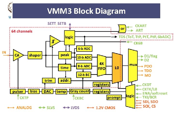
VMM 3 Block Diagram

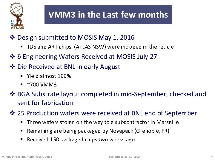
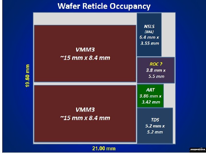
VMM 3 in the Last few months v Design submitted to MOSIS May 1, 2016 § TDS and ART chips (ATLAS NSW) were included in the reticle v 6 Engineering Wafers Received at MOSIS July 27 v Die Received at BNL in early August § Yield almost 100% § ~700 VMM 3 v BGA Substrate layout completed in mid-September, checked and sent for fabrication v 25 Production wafers were received at BNL end of September § Three wafers stolen on the way to a subcontractor in Marseille § Remaining are being packaged by Novapack (Grenoble, FR) § Received 150 packaged chips two weeks ago V. Polychronakos, Muon Week, Chios september 26 -31, 2016 4

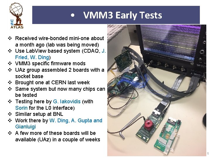
• VMM 3 Early Tests v Received wire-bonded mini-one about a month ago (lab was being moved) v Use Lab. View based system (CDAQ, J. Fried, W. Ding) v VMM 3 specific firmware mods v UAz group assembled 2 boards with a socket base v Brought one at CERN last week v Same system but now many chips can be tested v Testing here by G. Iakovidis (with Sorin for the L 0 interface) v Similar setup at BNL v Work there by W. Ding, A. Gupta and Gianluigi v A few more of these boards will be available (UAz) in a couple of weeks 5

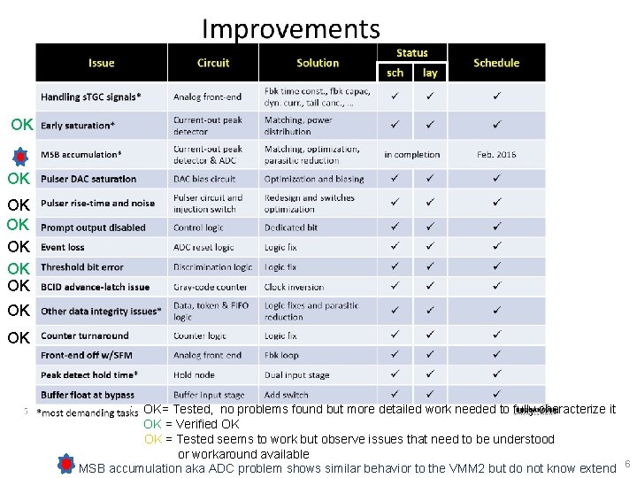
OK OK OK : OK= Tested, no problems found but more detailed work needed to fully characterize it OK = Verified OK OK = Tested seems to work but observe issues that need to be understood or workaround available MSB accumulation aka ADC problem shows similar behavior to the VMM 2 but do not know extend 6

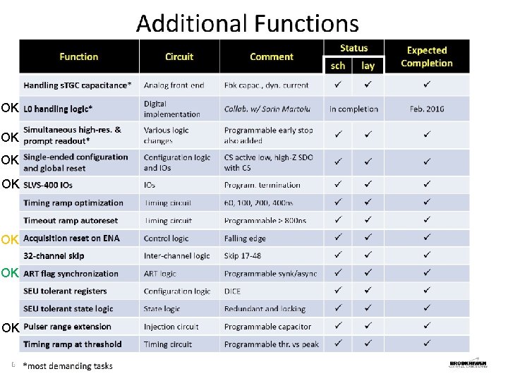
OK OK 7

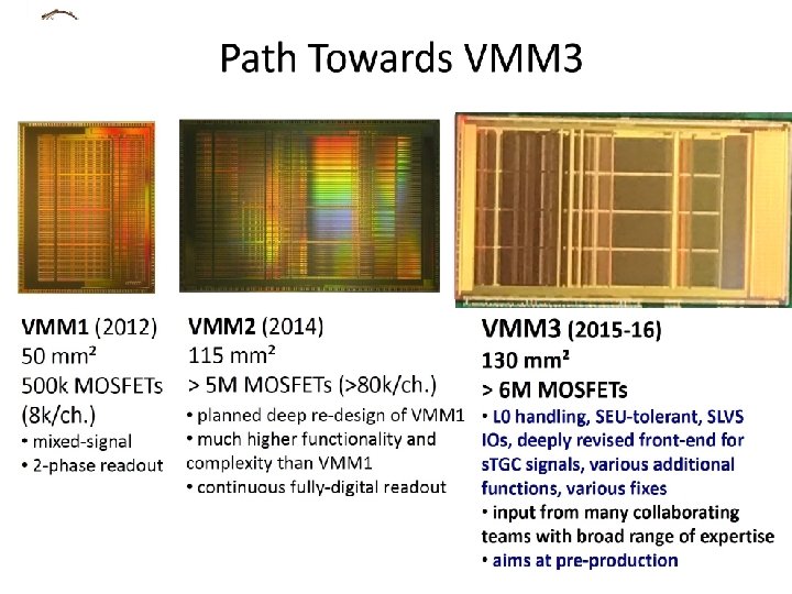
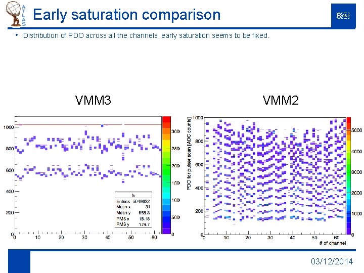
Early saturation comparison • 8 Distribution of PDO across all the channels, early saturation seems to be fixed. VMM 3 VMM 2 03/12/2014

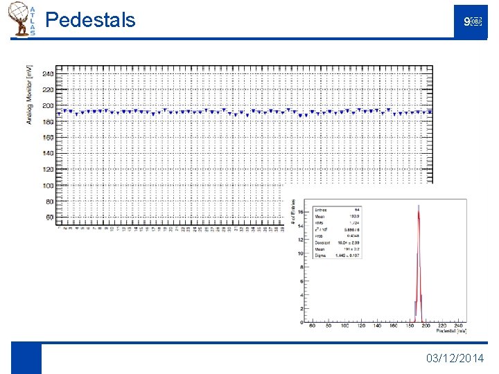
Pedestals 9 03/12/2014
![DACs VMM 3 10 Pulser m V vs DAC count VMM 3 DACs – VMM 3 10 Pulser [m. V] vs DAC count – VMM 3](https://slidetodoc.com/presentation_image_h2/5ce11f24dc65bee89d4621e9c6dbcd1a/image-10.jpg)
DACs – VMM 3 10 Pulser [m. V] vs DAC count – VMM 3 03/12/2014

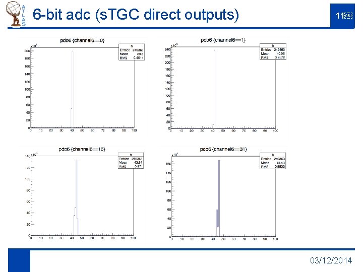
6 -bit adc (s. TGC direct outputs) 11 03/12/2014

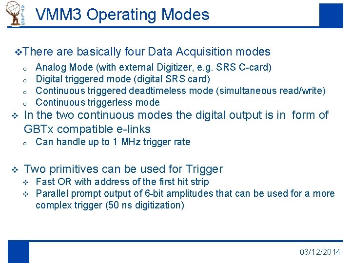
VMM 3 Operating Modes v. There o o v Analog Mode (with external Digitizer, e. g. SRS C-card) Digital triggered mode (digital SRS card) Continuous triggered deadtimeless mode (simultaneous read/write) Continuous triggerless mode In the two continuous modes the digital output is in form of GBTx compatible e-links o v are basically four Data Acquisition modes Can handle up to 1 MHz trigger rate Two primitives can be used for Trigger v v Fast OR with address of the first hit strip Parallel prompt output of 6 -bit amplitudes that can be used for a more complex trigger (50 ns digitization) 03/12/2014

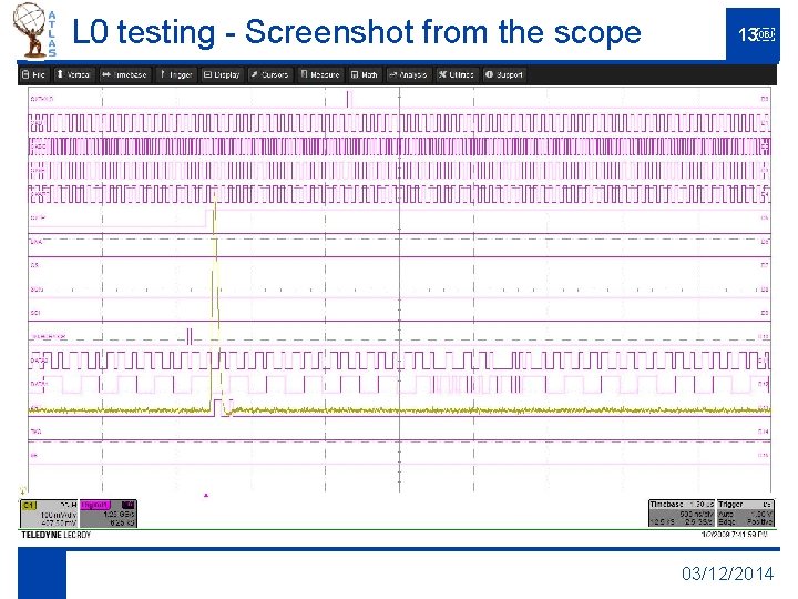
L 0 testing - Screenshot from the scope 13 03/12/2014

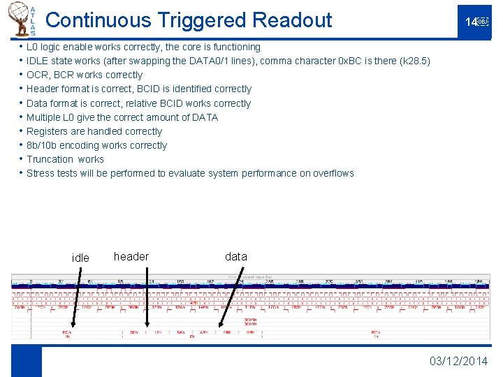
Continuous Triggered Readout 14 • L 0 logic enable works correctly, the core is functioning • IDLE state works (after swapping the DATA 0/1 lines), comma character 0 x. BC is there (k 28. 5) • OCR, BCR works correctly • Header format is correct, BCID is identified correctly • Data format is correct, relative BCID works correctly • Multiple L 0 give the correct amount of DATA • Registers are handled correctly • 8 b/10 b encoding works correctly • Truncation works • Stress tests will be performed to evaluate system performance on overflows idle header data 03/12/2014

15

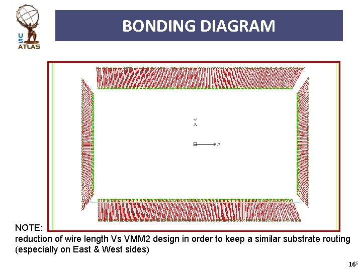
BONDING DIAGRAM NOTE: reduction of wire length Vs VMM 2 design in order to keep a similar substrate routing (especially on East & West sides) 1616

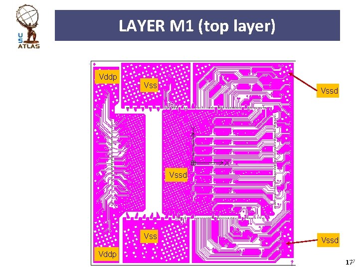
LAYER M 1 (top layer) Vddp Vssd Vss Vddp Vssd 1717

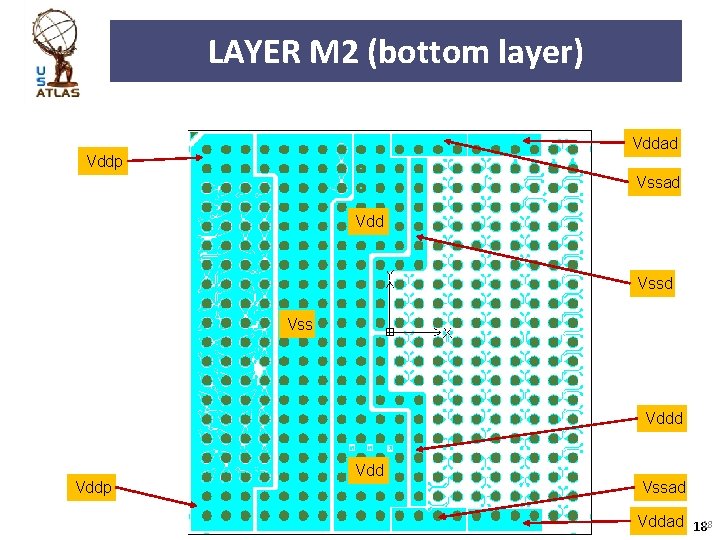
LAYER M 2 (bottom layer) Vddad Vddp Vssad Vdd Vss Vddd Vddp Vdd Vssad Vddad 1818

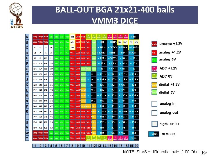
BALL-OUT BGA 21 x 21 -400 balls VMM 3 DICE NOTE: SLVS = differential pairs (100 Ohms)1919

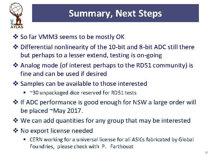
Summary, Next Steps v So far VMM 3 seems to be mostly OK v Differential nonlinearity of the 10 -bit and 8 -bit ADC still there but perhaps to a lesser extend, testing is on-going v Analog mode (of interest perhaps to the RD 51 community) is fine and can be used if desired v Samples can be available to those interested § ~30 unpackaged dice reserved for RD 51 tests v If ADC performance is good enough for NSW a large order will be placed ~May 2017. v We can add quantities for any group that may be interested v No export license needed § CERN working for a universal license for all ASICs fabricated by Global Foundries, please check with P. Farthouat 20