Santa Cruz Institute for Particle Physics SCIPP Evaluation
![Fluence [1014 neq/cm 2] Challenges for ATLAS Upgrade 10/26 Inner Pixel Mid-Radius Short Strips Fluence [1014 neq/cm 2] Challenges for ATLAS Upgrade 10/26 Inner Pixel Mid-Radius Short Strips](https://slidetodoc.com/presentation_image_h2/8d0455f98820458603bb271eb716ce0e/image-3.jpg)
- Slides: 11

Santa Cruz Institute for Particle Physics SCIPP Evaluation of the Radiation Tolerance of Si. Ge Heterojunction Bipolar Transistors Under 24 Ge. V Proton Exposure J. Metcalfe, D. E. Dorfan, A. A. Grillo, M Rogers, H. F. -W. Sadrozinski, A. Seiden, E. Spencer, M. Wilder SCIPP, University of California Santa Cruz, 95064, USA A. Sutton, G. Prakash, J. D. Cressler Georgia Tech, Atlanta, GA 30332 -0250, USA 10/26 Rad Tolerance of Si. Ge HBT J. Metcalfe

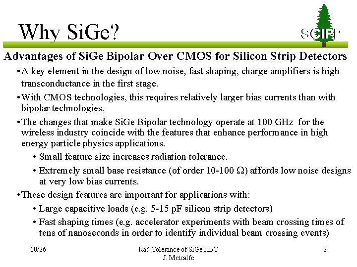
Why Si. Ge? SCIPP Advantages of Si. Ge Bipolar Over CMOS for Silicon Strip Detectors • A key element in the design of low noise, fast shaping, charge amplifiers is high transconductance in the first stage. • With CMOS technologies, this requires relatively larger bias currents than with bipolar technologies. • The changes that make Si. Ge Bipolar technology operate at 100 GHz for the wireless industry coincide with the features that enhance performance in high energy particle physics applications. • Small feature size increases radiation tolerance. • Extremely small base resistance (of order 10 -100 W) affords low noise designs at very low bias currents. • These design features are important for applications with: • Large capacitive loads (e. g. 5 -15 p. F silicon strip detectors) • Fast shaping times (e. g. accelerator experiments with beam crossing times of tens of nanoseconds in order to identify individual beam crossing events) 10/26 Rad Tolerance of Si. Ge HBT J. Metcalfe 2
![Fluence 1014 neqcm 2 Challenges for ATLAS Upgrade 1026 Inner Pixel MidRadius Short Strips Fluence [1014 neq/cm 2] Challenges for ATLAS Upgrade 10/26 Inner Pixel Mid-Radius Short Strips](https://slidetodoc.com/presentation_image_h2/8d0455f98820458603bb271eb716ce0e/image-3.jpg)
Fluence [1014 neq/cm 2] Challenges for ATLAS Upgrade 10/26 Inner Pixel Mid-Radius Short Strips Outer-Radius “SCT” SCIPP • The LHC upgrade will increase the luminosity by a factor of 10! Fluences in the inner detector will reach as high as 1016 neq/cm 2! • The challenge is to find front -end electronics resistant to radiation damage that will also reduce power consumption with acceptable noise. • Our efforts focus on fluences achieved in the mid to outer radii of silicon strip detectors. Rad Tolerance of Si. Ge HBT J. Metcalfe 3

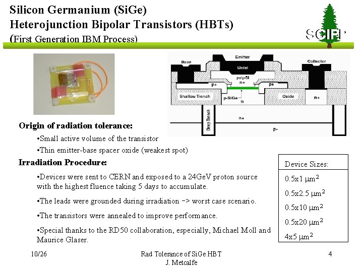
Silicon Germanium (Si. Ge) Heterojunction Bipolar Transistors (HBTs) (First Generation IBM Process) SCIPP Origin of radiation tolerance: • Small active volume of the transistor • Thin emitter-base spacer oxide (weakest spot) Irradiation Procedure: Device Sizes: • Devices were sent to CERN and exposed to a 24 Ge. V proton source with the highest fluence taking 5 days to accumulate. • The leads were grounded during irradiation --> worst case scenario. • The transistors were annealed to improve performance. • Special thanks to the RD 50 collaboration, especially, Michael Moll and Maurice Glaser. 10/26 Rad Tolerance of Si. Ge HBT J. Metcalfe 0. 5 x 1 mm 2 0. 5 x 2. 5 mm 2 0. 5 x 10 mm 2 0. 5 x 20 mm 2 4 x 5 mm 2 4

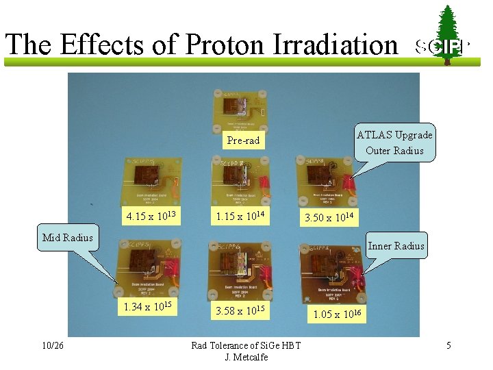
The Effects of Proton Irradiation ATLAS Upgrade Outer Radius Pre-rad 4. 15 x 1013 1. 15 x 1014 3. 50 x 1014 Mid Radius Inner Radius 1. 34 x 1015 10/26 SCIPP 3. 58 x 1015 Rad Tolerance of Si. Ge HBT J. Metcalfe 1. 05 x 1016 5

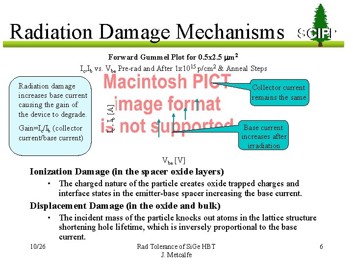
Radiation Damage Mechanisms SCIPP Forward Gummel Plot for 0. 5 x 2. 5 mm 2 Ic, Ib vs. Vbe Pre-rad and After 1 x 10¹⁵ p/cm 2 & Anneal Steps Gain=Ic/Ib (collector current/base current) Collector current remains the same Ic , Ib [A] Radiation damage increases base current causing the gain of the device to degrade. Base current increases after irradiation Vbe [V] Ionization Damage (in the spacer oxide layers) • The charged nature of the particle creates oxide trapped charges and interface states in the emitter-base spacer increasing the base current. Displacement Damage (in the oxide and bulk) • The incident mass of the particle knocks out atoms in the lattice structure shortening hole lifetime, which is inversely proportional to the base current. 10/26 Rad Tolerance of Si. Ge HBT J. Metcalfe 6

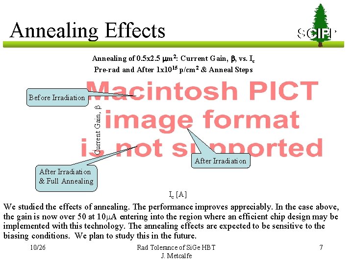
Annealing Effects SCIPP Annealing of 0. 5 x 2. 5 mm 2: Current Gain, b, vs. Ic Pre-rad and After 1 x 10¹⁵ p/cm 2 & Anneal Steps Current Gain, b Before Irradiation After Irradiation & Full Annealing Ic [A] We studied the effects of annealing. The performance improves appreciably. In the case above, the gain is now over 50 at 10 m. A entering into the region where an efficient chip design may be implemented with this technology. The annealing effects are expected to be sensitive to the biasing conditions. We plan to study this in the future. 10/26 Rad Tolerance of Si. Ge HBT J. Metcalfe 7

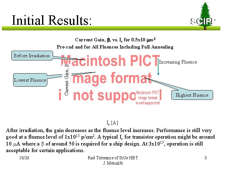
Initial Results: SCIPP Current Gain, b, vs. Ic for 0. 5 x 10 mm 2 Pre-rad and for All Fluences Including Full Annealing Before Irradiation Current Gain, bb Current Lowest Fluence Increasing Fluence Highest Fluence Ic [A] After irradiation, the gain decreases as the fluence level increases. Performance is still very good at a fluence level of 1 x 10¹⁵ p/cm 2. A typical Ic for transistor operation might be around 10 m. A where a b of around 50 is required for a chip design. At 3 x 10¹⁵, operation is still acceptable for certain applications. 10/26 Rad Tolerance of Si. Ge HBT J. Metcalfe 8

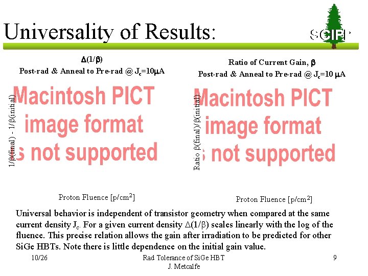
Universality of Results: Ratio of Current Gain, b Post-rad & Anneal to Pre-rad @ Jc=10 m. A Ratio b(final)/b(initial) 1/b(final) - 1/b(initial) D(1/b) Post-rad & Anneal to Pre-rad @ Jc=10 m. A SCIPP Proton Fluence [p/cm 2] Universal behavior is independent of transistor geometry when compared at the same current density Jc. For a given current density D(1/b) scales linearly with the log of the fluence. This precise relation allows the gain after irradiation to be predicted for other Si. Ge HBTs. Note there is little dependence on the initial gain value. 10/26 Rad Tolerance of Si. Ge HBT J. Metcalfe 9

Feasibility for ATLAS Inner Detector Upgrade SCIPP Qualifications for a good transistor: • A gain of 50 is a good figure of merit for a transistor to use in a front-end circuit design. • Low currents translate into increased power savings. At 3. 5 x 10¹⁴ in the outer region (60 cm), where long (10 cm) silicon strip detectors with capacitances around 15 p. F will be used, the collector current Ic is low enough for substantial power savings over CMOS! 10/26 At 1. 34 x 1015 closer to the mid radius (20 cm), where short (3 cm) silicon strip detectors with capacitance around 5 p. F will be used, the collector current Ic is still good for a front transistor, which requires a larger current while minimizing noise. We expect better results from 3 rd generation IBM Si. Ge HBTs. Rad Tolerance of Si. Ge HBT J. Metcalfe 10

Conclusions SCIPP • We extended the radiation testing of Si. Ge Bipolar transistors by a factor 100 in fluence thanks to the RD 50 radiation program. • The 5 HP technology we examined is far superior to that used for the current ATLAS silicon strip detectors. • The 5 HP demonstrates utility--power savings and low noise--for the entire analog front-end in the outer region and for the front transistor in the mid radius of ATLAS Upgrade. • Future generations (smaller sizes) of Si. Ge HBTs show huge potential for power savings with low noise at extreme radiation levels. • Investigation is currently under way to determine the benefits of the next generations of Si. Ge HBTs in future collider experiments (i. e. s. LHC). 10/26 Rad Tolerance of Si. Ge HBT J. Metcalfe 11