Retiming Consider the Following Circuit Suppose TXOR 3
- Slides: 15
Retiming
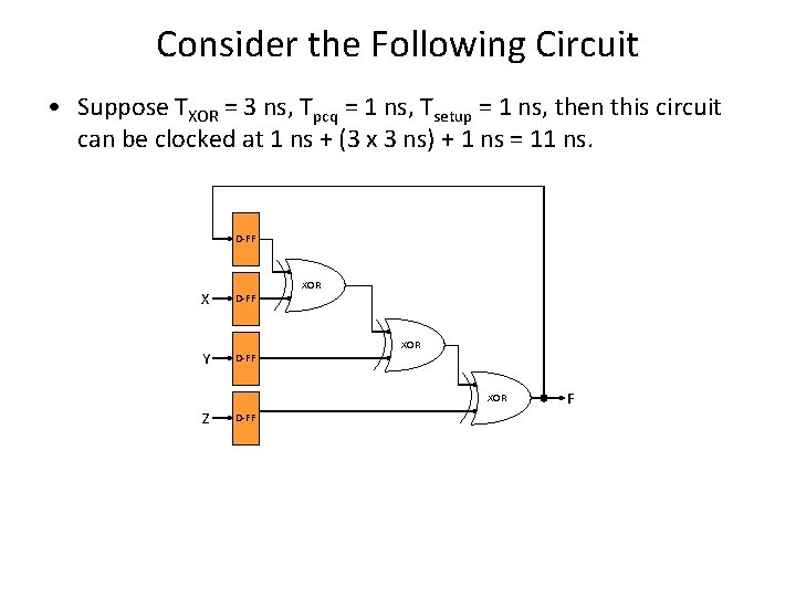
Consider the Following Circuit • Suppose TXOR = 3 ns, Tpcq = 1 ns, Tsetup = 1 ns, then this circuit can be clocked at 1 ns + (3 x 3 ns) + 1 ns = 11 ns. D-FF X D-FF Y D-FF XOR XOR Z D-FF F
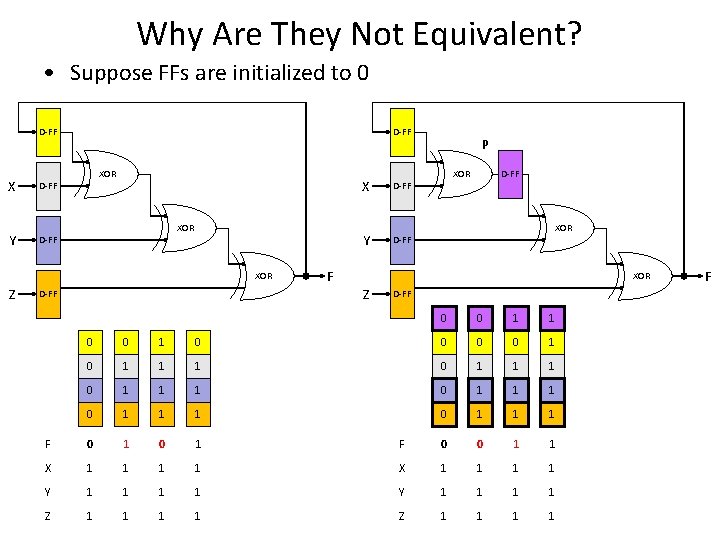
Why Are They Not Equivalent? • Suppose FFs are initialized to 0 D-FF X D-FF Y D-FF XOR XOR Z X D-FF Y D-FF XOR Z D-FF P D-FF 0 0 1 1 0 0 0 0 1 1 1 0 1 1 1 F 0 1 F 0 0 1 1 X 1 1 1 1 Y 1 1 1 1 Z 1 1 1 1 F
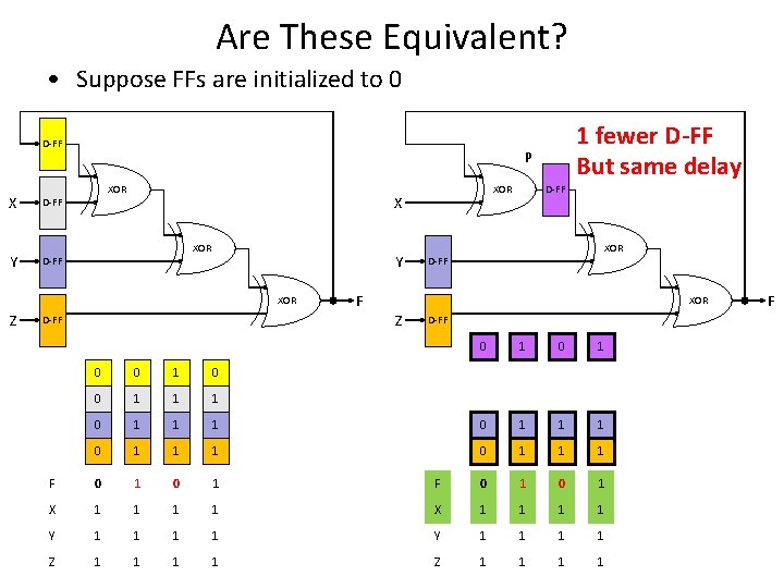
Are These Equivalent? • Suppose FFs are initialized to 0 D-FF X D-FF Y D-FF P XOR X XOR Y XOR Z 1 fewer D-FF But same delay XOR D-FF F XOR Z D-FF 0 1 0 0 1 1 1 0 1 1 1 F 0 1 0 1 X 1 1 1 1 Y 1 1 1 1 Z 1 1 1 1 F
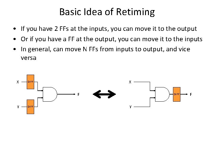
Basic Idea of Retiming • If you have 2 FFs at the inputs, you can move it to the output • Or if you have a FF at the output, you can move it to the inputs • In general, can move N FFs from inputs to output, and vice versa X X D-FF F Y D-FF Y F
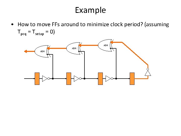
Example • How to move FFs around to minimize clock period? (assuming Tpcq = Tsetup = 0) XOR XOR
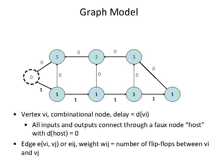
Graph Model 0 0 3 3 1 1 3 0 0 1 1 • Vertex vi, combinational node, delay = d(vi) • All inputs and outputs connect through a faux node “host” with d(host) = 0 • Edge e(vi, vj) or eij, weight wij = number of flip-flops between vi and vj
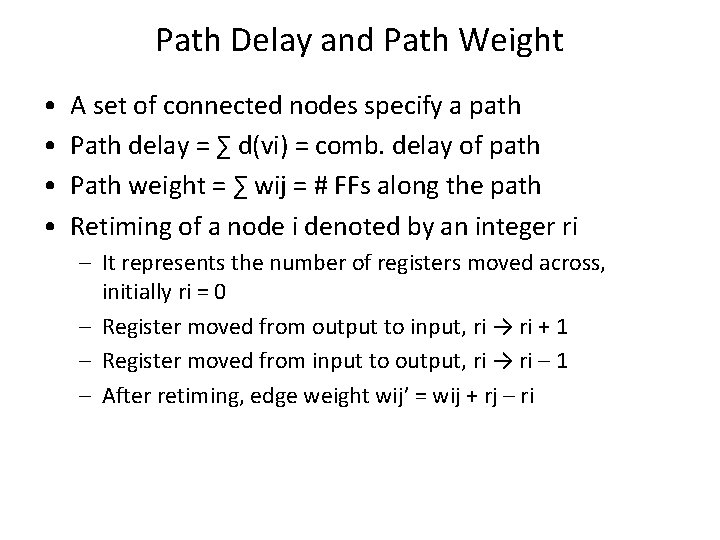
Path Delay and Path Weight • • A set of connected nodes specify a path Path delay = ∑ d(vi) = comb. delay of path Path weight = ∑ wij = # FFs along the path Retiming of a node i denoted by an integer ri – It represents the number of registers moved across, initially ri = 0 – Register moved from output to input, ri → ri + 1 – Register moved from input to output, ri → ri – 1 – After retiming, edge weight wij’ = wij + rj – ri
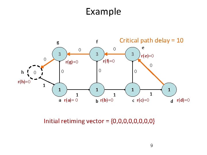
Example 0 h r(h)=0 0 3 1 a r(a)= 0 3 0 0 1 e r(e)=0 r(f)=0 r(g)=0 0 1 Critical path delay = 10 f g 1 b r(b)=0 0 1 1 c r(c)=0 0 1 Initial retiming vector = {0, 0, 0} 9 1 d r(d)=0
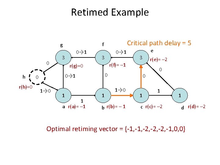
Retimed Example 0 h r(h)=0 0→ 1 3 1 a r(a)= – 1 3 0 0→ 1 1 e r(e)= – 2 r(f)= – 1 r(g)=0 0 1→ 0 Critical path delay = 5 f g 1 0 1→ 0 b r(b)= – 1 1 0 1 c r(c)= – 2 1 d r(d)= – 2 Optimal retiming vector = {-1, -2, -2, -1, 0, 0}
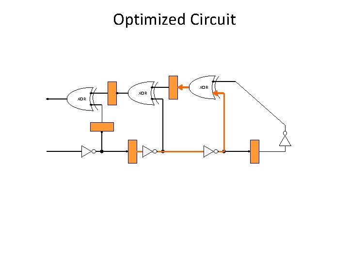
Optimized Circuit XOR XOR
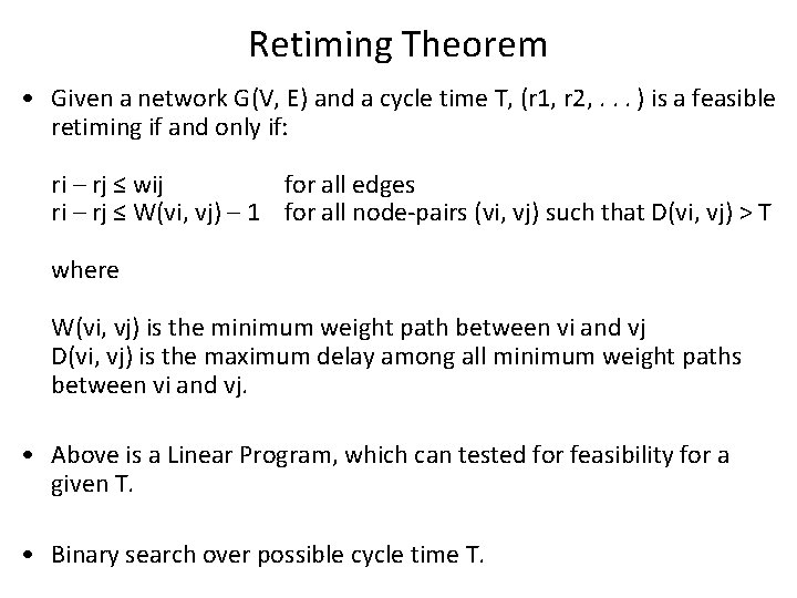
Retiming Theorem • Given a network G(V, E) and a cycle time T, (r 1, r 2, . . . ) is a feasible retiming if and only if: ri – rj ≤ wij for all edges ri – rj ≤ W(vi, vj) – 1 for all node-pairs (vi, vj) such that D(vi, vj) > T where W(vi, vj) is the minimum weight path between vi and vj D(vi, vj) is the maximum delay among all minimum weight paths between vi and vj. • Above is a Linear Program, which can tested for feasibility for a given T. • Binary search over possible cycle time T.
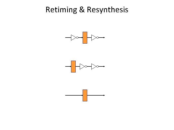
Retiming & Resynthesis
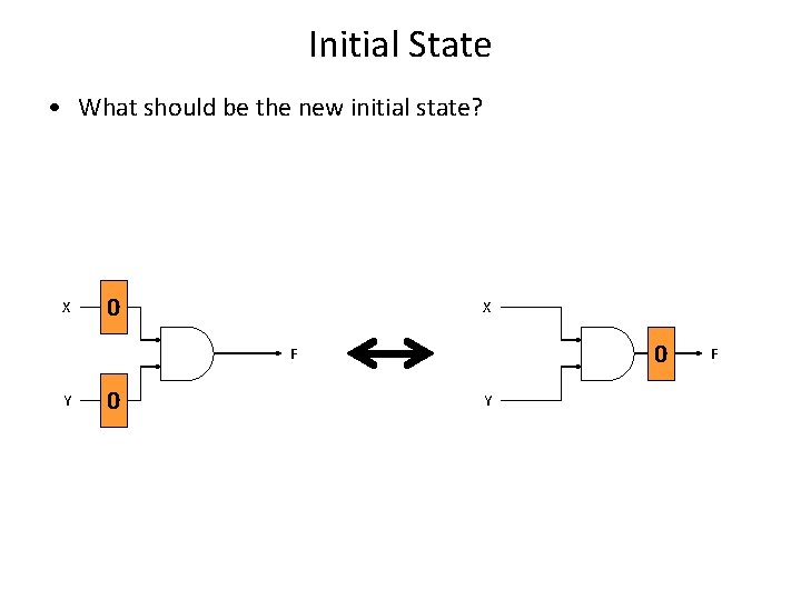
Initial State • What should be the new initial state? X 0 F Y 0 Y F
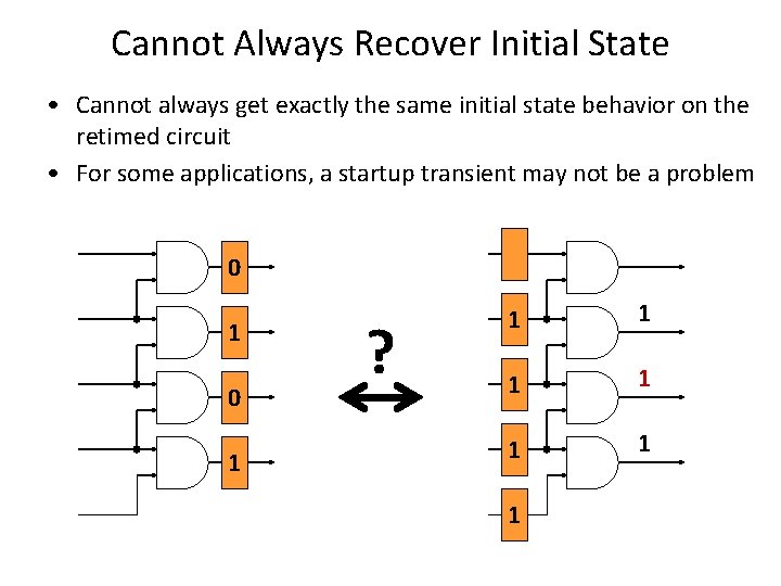
Cannot Always Recover Initial State • Cannot always get exactly the same initial state behavior on the retimed circuit • For some applications, a startup transient may not be a problem 0 1 ? 1 1 1 1