Quantum Mechanics and SpinValves Thomas Prevenslik QED Radiations
- Slides: 17

Quantum Mechanics and Spin-Valves Thomas Prevenslik QED Radiations Discovery Bay, Hong Kong 1 The 13 th IEEE Inter. Conf. on Nanotechnology, August 5 -8, Beijing, China 2013

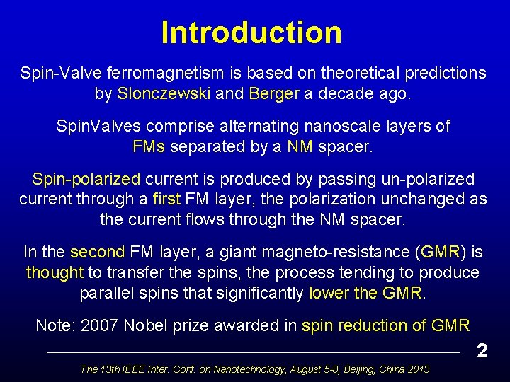
Introduction Spin-Valve ferromagnetism is based on theoretical predictions by Slonczewski and Berger a decade ago. Spin. Valves comprise alternating nanoscale layers of FMs separated by a NM spacer. Spin-polarized current is produced by passing un-polarized current through a first FM layer, the polarization unchanged as the current flows through the NM spacer. In the second FM layer, a giant magneto-resistance (GMR) is thought to transfer the spins, the process tending to produce parallel spins that significantly lower the GMR. Note: 2007 Nobel prize awarded in spin reduction of GMR 2 The 13 th IEEE Inter. Conf. on Nanotechnology, August 5 -8, Beijing, China 2013

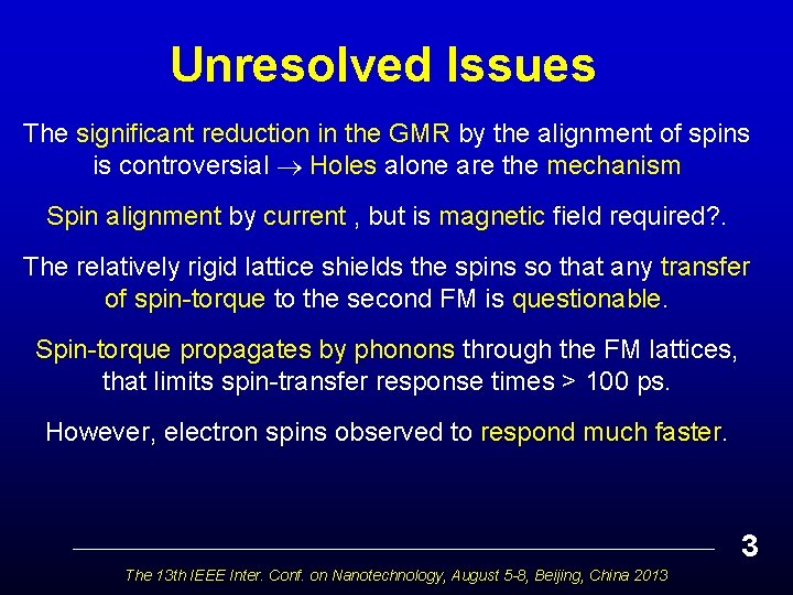
Unresolved Issues The significant reduction in the GMR by the alignment of spins is controversial Holes alone are the mechanism Spin alignment by current , but is magnetic field required? . The relatively rigid lattice shields the spins so that any transfer of spin-torque to the second FM is questionable. Spin-torque propagates by phonons through the FM lattices, that limits spin-transfer response times > 100 ps. However, electron spins observed to respond much faster. 3 The 13 th IEEE Inter. Conf. on Nanotechnology, August 5 -8, Beijing, China 2013

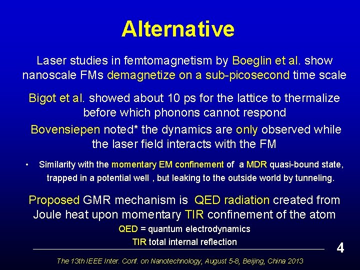
Alternative Laser studies in femtomagnetism by Boeglin et al. show nanoscale FMs demagnetize on a sub-picosecond time scale Bigot et al. showed about 10 ps for the lattice to thermalize before which phonons cannot respond Bovensiepen noted* the dynamics are only observed while the laser field interacts with the FM • Similarity with the momentary EM confinement of a MDR quasi-bound state, trapped in a potential well , but leaking to the outside world by tunneling. Proposed GMR mechanism is QED radiation created from Joule heat upon momentary TIR confinement of the atom QED = quantum electrodynamics TIR total internal reflection The 13 th IEEE Inter. Conf. on Nanotechnology, August 5 -8, Beijing, China 2013 4

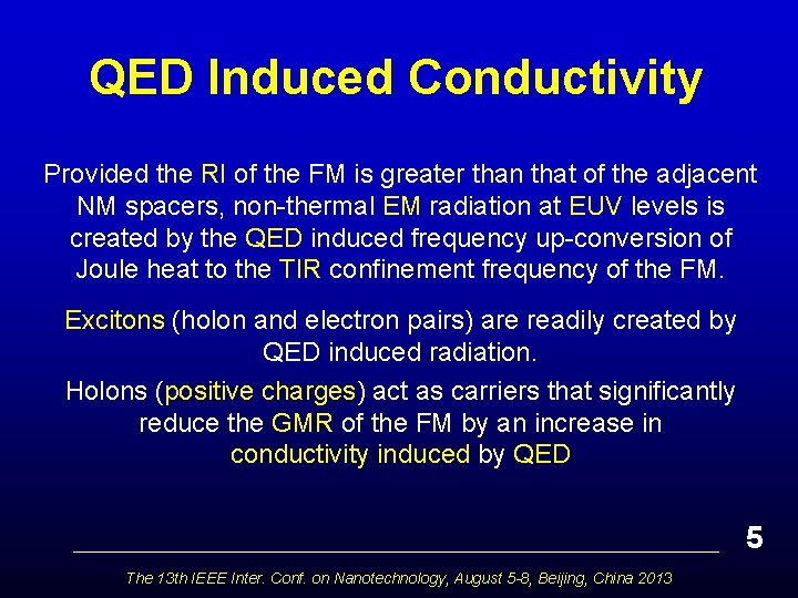
QED Induced Conductivity Provided the RI of the FM is greater than that of the adjacent NM spacers, non-thermal EM radiation at EUV levels is created by the QED induced frequency up-conversion of Joule heat to the TIR confinement frequency of the FM. Excitons (holon and electron pairs) are readily created by QED induced radiation. Holons (positive charges) act as carriers that significantly reduce the GMR of the FM by an increase in conductivity induced by QED 5 The 13 th IEEE Inter. Conf. on Nanotechnology, August 5 -8, Beijing, China 2013

Theory Heat Capacity of the Atom Conservation of Energy TIR Confinement 6 The 13 th IEEE Inter. Conf. on Nanotechnology, August 5 -8, Beijing, China 2013

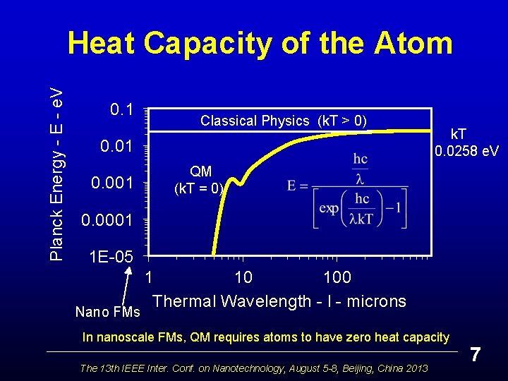
Planck Energy - E - e. V Heat Capacity of the Atom 0. 1 Classical Physics (k. T > 0) 0. 01 0. 001 k. T 0. 0258 e. V QM (k. T = 0) 0. 0001 1 E-05 Nano FMs 1 10 100 Thermal Wavelength - l - microns In nanoscale FMs, QM requires atoms to have zero heat capacity The 13 th IEEE Inter. Conf. on Nanotechnology, August 5 -8, Beijing, China 2013 7

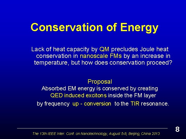
Conservation of Energy Lack of heat capacity by QM precludes Joule heat conservation in nanoscale FMs by an increase in temperature, but how does conservation proceed? Proposal Absorbed EM energy is conserved by creating QED induced excitons inside the FM layer by frequency up - conversion to the TIR resonance. The 13 th IEEE Inter. Conf. on Nanotechnology, August 5 -8, Beijing, China 2013 8

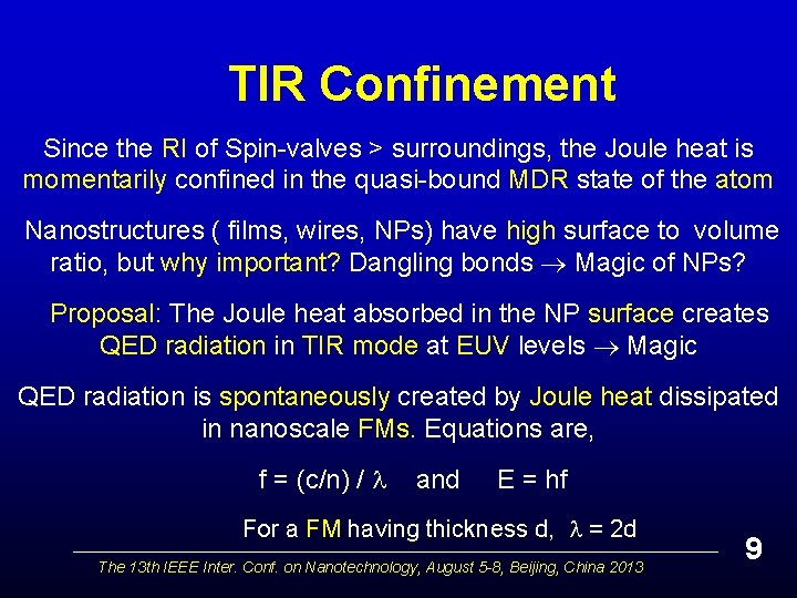
TIR Confinement Since the RI of Spin-valves > surroundings, the Joule heat is momentarily confined in the quasi-bound MDR state of the atom Nanostructures ( films, wires, NPs) have high surface to volume ratio, but why important? Dangling bonds Magic of NPs? Proposal: The Joule heat absorbed in the NP surface creates QED radiation in TIR mode at EUV levels Magic QED radiation is spontaneously created by Joule heat dissipated in nanoscale FMs. Equations are, f = (c/n) / and E = hf For a FM having thickness d, = 2 d The 13 th IEEE Inter. Conf. on Nanotechnology, August 5 -8, Beijing, China 2013 9

Electrical Response QED Photons and Excitons Exciton Response Resistance and Current 10 The 13 th IEEE Inter. Conf. on Nanotechnology, August 5 -8, Beijing, China 2013

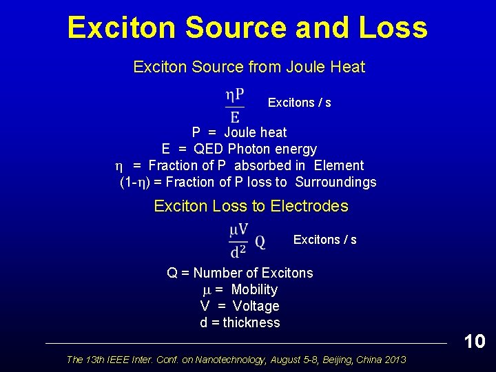
Exciton Source and Loss Exciton Source from Joule Heat Excitons / s P = Joule heat E = QED Photon energy = Fraction of P absorbed in Element (1 - ) = Fraction of P loss to Surroundings Exciton Loss to Electrodes Excitons / s Q = Number of Excitons = Mobility V = Voltage d = thickness 10 The 13 th IEEE Inter. Conf. on Nanotechnology, August 5 -8, Beijing, China 2013

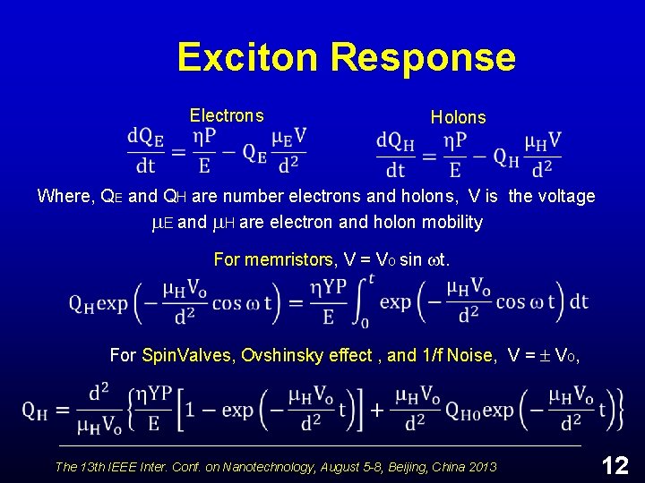
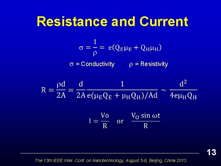
Exciton Response Electrons Holons Where, QE and QH are number electrons and holons, V is the voltage E and H are electron and holon mobility For memristors, V = Vo sin t. For Spin. Valves, Ovshinsky effect , and 1/f Noise, V = Vo, The 13 th IEEE Inter. Conf. on Nanotechnology, August 5 -8, Beijing, China 2013 12

Resistance and Current = Conductivity = Resistivity 13 The 13 th IEEE Inter. Conf. on Nanotechnology, August 5 -8, Beijing, China 2013

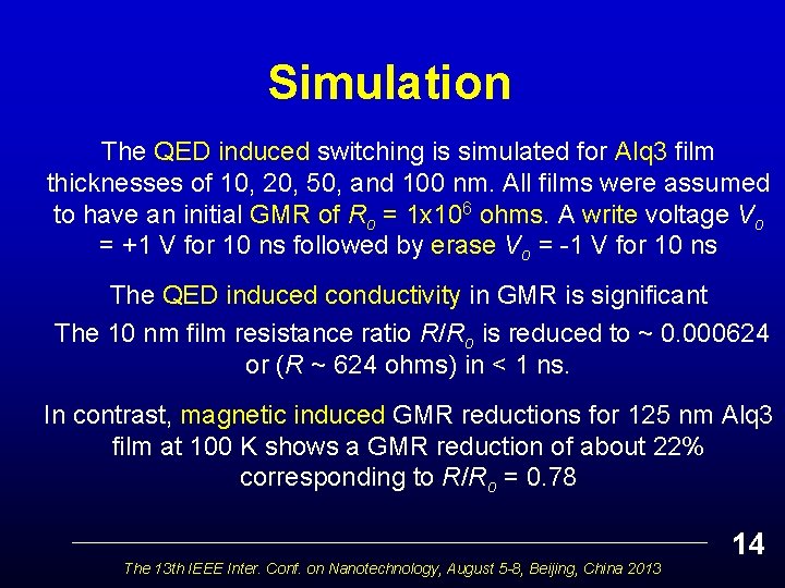
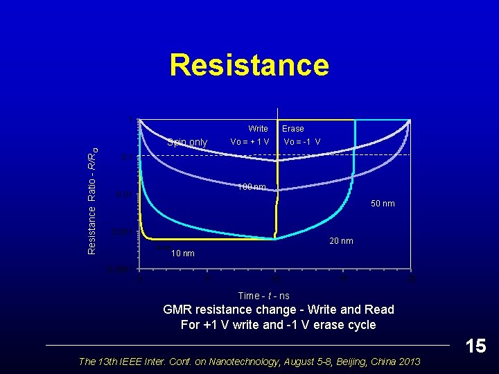
Simulation The QED induced switching is simulated for Alq 3 film thicknesses of 10, 20, 50, and 100 nm. All films were assumed to have an initial GMR of Ro = 1 x 10⁶ ohms. A write voltage Vo = +1 V for 10 ns followed by erase Vo = -1 V for 10 ns The QED induced conductivity in GMR is significant The 10 nm film resistance ratio R/Ro is reduced to ~ 0. 000624 or (R ~ 624 ohms) in < 1 ns. In contrast, magnetic induced GMR reductions for 125 nm Alq 3 film at 100 K shows a GMR reduction of about 22% corresponding to R/Ro = 0. 78 The 13 th IEEE Inter. Conf. on Nanotechnology, August 5 -8, Beijing, China 2013 14

Resistance 1 Write Erase Resistance Ratio - R/RO Spin only Vo = + 1 V Vo = -1 V 0. 1 100 nm 0. 01 50 nm 0. 001 10 nm 20 nm 10 nm 0. 0001 0 5 10 15 20 Time - t - ns GMR resistance change - Write and Read For +1 V write and -1 V erase cycle The 13 th IEEE Inter. Conf. on Nanotechnology, August 5 -8, Beijing, China 2013 15

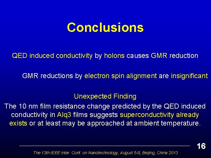
Conclusions QED induced conductivity by holons causes GMR reduction GMR reductions by electron spin alignment are insignificant Unexpected Finding The 10 nm film resistance change predicted by the QED induced conductivity in Alq 3 films suggests superconductivity already exists or at least may be approached at ambient temperature. The 13 th IEEE Inter. Conf. on Nanotechnology, August 5 -8, Beijing, China 2013 16

Questions & Papers Email: nanoqed@gmail. com http: //www. nanoqed. org 17 The 13 th IEEE Inter. Conf. on Nanotechnology, August 5 -8, Beijing, China 2013