PLAsPALs and PLA Design Optimization Shantanu Dutt Electerical
- Slides: 15

PLAs/PALs and PLA Design Optimization Shantanu Dutt Electerical and Computer Engr. Univ. of Illinois at Chicago

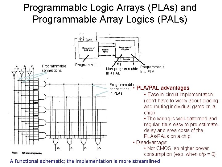
Programmable Logic Arrays (PLAs) and Programmable Array Logics (PALs) Programmable connections Programmable Non-programmable Programmable In a PLA In a PAL Programmable connections • in PLAs PLA/PAL advantages • Ease in circuit implementation (don’t have to worry about placing and routing individual gates on a chip) • The wiring is well-patterned and regular; thus easy to pre-estimate delay and area costs of the PLAs/PALs on a chip • Disadvantage: • Not CMOS, so higher power consumption (esp. when o/p = 0) A functional schematic; the implementation is more streamlined

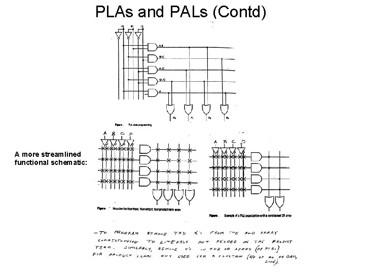
PLAs and PALs (Contd) A more streamlined functional schematic:

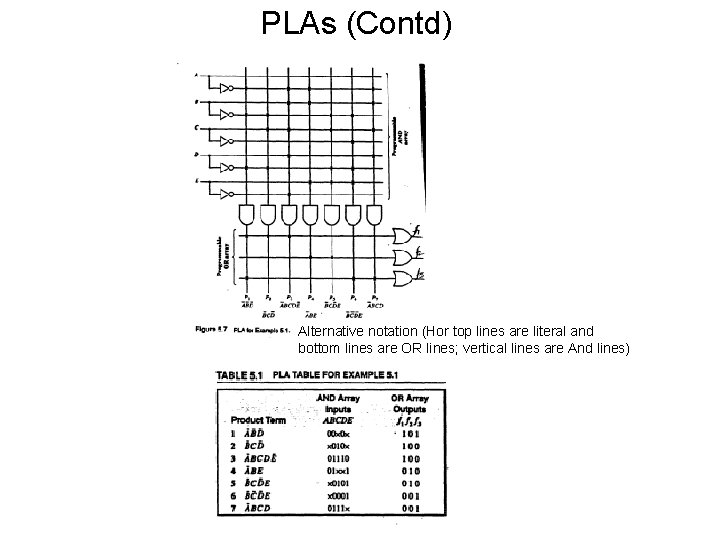
PLAs (Contd) Alternative notation (Hor top lines are literal and bottom lines are OR lines; vertical lines are And lines)

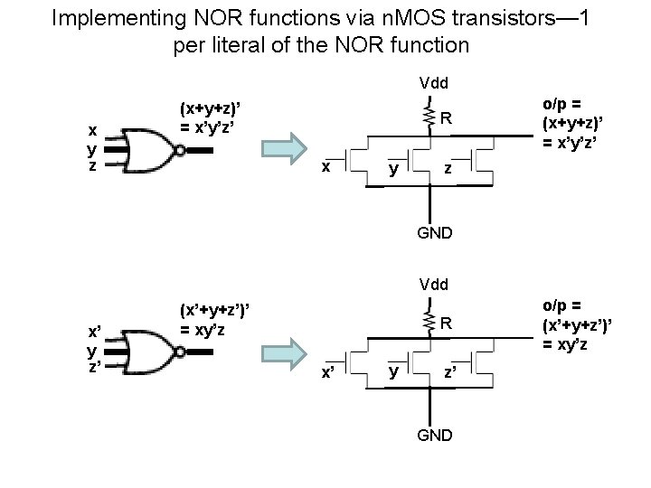
Implementing NOR functions via n. MOS transistors— 1 per literal of the NOR function Vdd x y z (x+y+z)’ = x’y’z’ R x y o/p = (x+y+z)’ = x’y’z’ z GND Vdd x’ y z’ (x’+y+z’)’ = xy’z R x’ y z’ GND o/p = (x’+y+z’)’ = xy’z

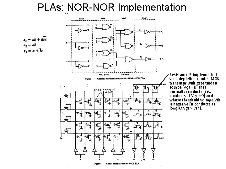
PLAs: NOR-NOR Implementation Resistance R implemented via a depletion-mode n. MOS transistor with gate tied to source [Vgs = 0] that normally conducts [i. e. , conducts at Vgs = 0] and whose threshold voltage Vth is negative [it conducts as long as Vgs > Vth].

PLAs (Contd)

PLAs (Contd)

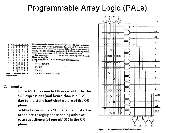
Programmable Array Logic (PALs) Comments: • More AND lines needed than called for by the SOP expressions (and hence than in a PLA) due to the static hardwired nature of the OR plane. • A little faster in the AND plane than PLAs due to the pre-charging phase seeing only one gate capacitance (of one n. MOS) in the OR plane.

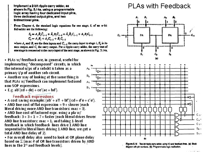
PLAs with Feedback • PLAs w/ feedback are, in general, useful for implementing “decomposed” circuits, in which the internal o/ps of a subckt is taken as a primary i/p of another sub-circuit. • Another way of looking at the same thing is that PLAs w/ feedback can implement factored non-SOP expressions. • E. g. ab’(cd + de) + ce’(ac + bd’). A 0 B 0 A 1 B 1 Feedback expressions • A cost saving example: (ab’ + a’f + bf’)(cd + d’e + c’e’). • AND line cost of flat expression = 9 + slower (each literal driving more AND line transistors: max = 3). • AND line cost of factored expr. using a pla w/ feedback: 3 + 1 = 7 + faster (each literal drives fewer AND line transistors: max = 1, and taking 1 -level feedback in which feedback lines drive 1 AND line sequential to literal lines driving 1 AND line, we get a total AND line delay of 2). • For overall delay also need to look at OR plane delay based on S [max # of OR line transistors driven by AND lines in the 1 st and feedback levels]. C-1 C 0 C 1 S 0 S 1

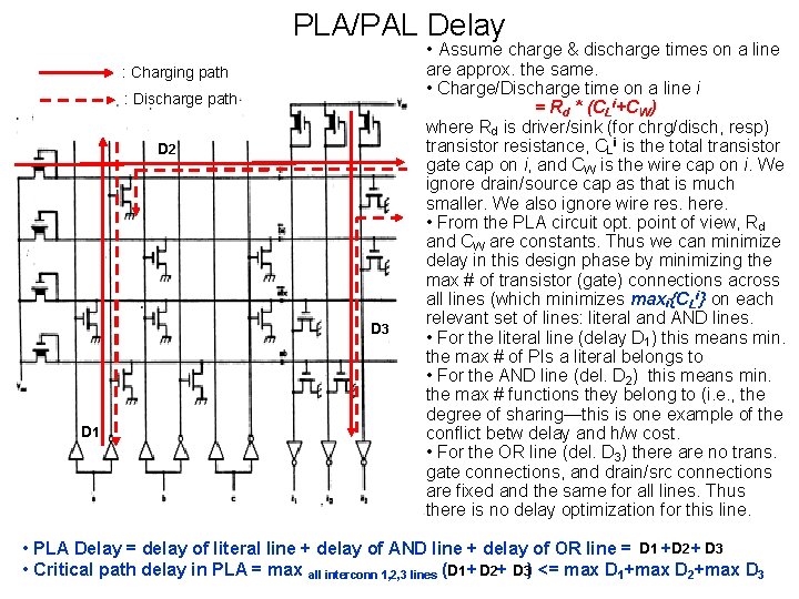
PLA/PAL Delay • Assume charge & discharge times on a line : Charging path : Discharge path D 2 D 3 D 1 are approx. the same. • Charge/Discharge time on a line i = Rd * (CLi+CW) where Rd is driver/sink (for chrg/disch, resp) transistor resistance, CLi is the total transistor gate cap on i, and CW is the wire cap on i. We ignore drain/source cap as that is much smaller. We also ignore wire res. here. • From the PLA circuit opt. point of view, Rd and CW are constants. Thus we can minimize delay in this design phase by minimizing the max # of transistor (gate) connections across all lines (which minimizes maxi{CLi} on each relevant set of lines: literal and AND lines. • For the literal line (delay D 1) this means min. the max # of PIs a literal belongs to • For the AND line (del. D 2) this means min. the max # functions they belong to (i. e. , the degree of sharing—this is one example of the conflict betw delay and h/w cost. • For the OR line (del. D 3) there are no trans. gate connections, and drain/src connections are fixed and the same for all lines. Thus there is no delay optimization for this line. • PLA Delay = delay of literal line + delay of AND line + delay of OR line = D 1 +D 2 + D 3 • Critical path delay in PLA = max all interconn 1, 2, 3 lines (D 1 + D 2+ D 3) <= max D 1+max D 2+max D 3

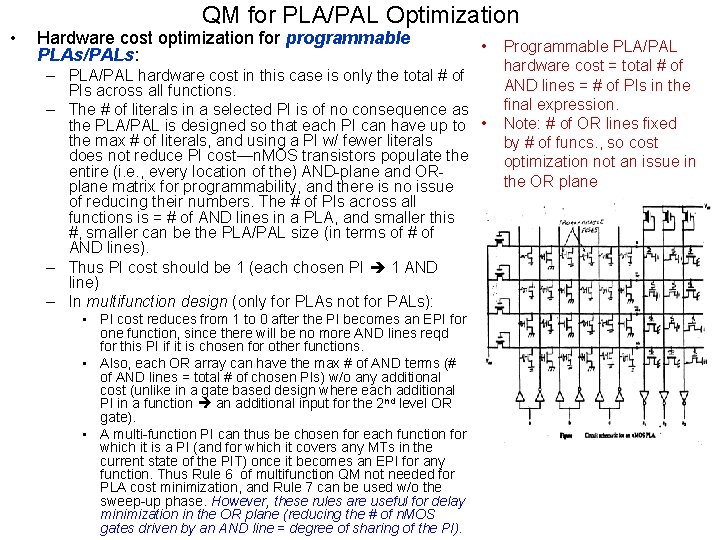
• QM for PLA/PAL Optimization Hardware cost optimization for programmable PLAs/PALs: • – PLA/PAL hardware cost in this case is only the total # of PIs across all functions. – The # of literals in a selected PI is of no consequence as the PLA/PAL is designed so that each PI can have up to • the max # of literals, and using a PI w/ fewer literals does not reduce PI cost—n. MOS transistors populate the entire (i. e. , every location of the) AND-plane and ORplane matrix for programmability, and there is no issue of reducing their numbers. The # of PIs across all functions is = # of AND lines in a PLA, and smaller this #, smaller can be the PLA/PAL size (in terms of # of AND lines). – Thus PI cost should be 1 (each chosen PI 1 AND line) – In multifunction design (only for PLAs not for PALs): • PI cost reduces from 1 to 0 after the PI becomes an EPI for one function, since there will be no more AND lines reqd for this PI if it is chosen for other functions. • Also, each OR array can have the max # of AND terms (# of AND lines = total # of chosen PIs) w/o any additional cost (unlike in a gate based design where each additional PI in a function an additional input for the 2 nd level OR gate). • A multi-function PI can thus be chosen for each function for which it is a PI (and for which it covers any MTs in the current state of the PIT) once it becomes an EPI for any function. Thus Rule 6 of multifunction QM not needed for PLA cost minimization, and Rule 7 can be used w/o the sweep-up phase. However, these rules are useful for delay minimization in the OR plane (reducing the # of n. MOS gates driven by an AND line = degree of sharing of the PI). Programmable PLA/PAL hardware cost = total # of AND lines = # of PIs in the final expression. Note: # of OR lines fixed by # of funcs. , so cost optimization not an issue in the OR plane

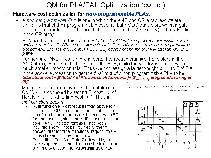
QM for PLA/PAL Optimization (contd. ) • Hardware cost optimization for non-programmable PLAs: – A non-programmable PLA is one in which the AND and OR array layouts are similar to that of their programmable cousins, but n. MOS transistors w/ their gate connections hardwired to the needed literal line (in the AND array) or the AND line in the OR array – PLA hardware cost in this case could be: total literal cost (= total # of transistors in the AND array) + total # of PIs across all functions (= # of AND lines corresponding transistors, one per AND line, in the OR array) + S each PI PIj [degree of sharing of PIj] (= total trans’s. in OR plane) – Further, # of AND lines is more important to reduce than # of transistors in the AND plane, as its affects the area of the PLA, while the # of transistors have a much smaller impact on this). Thus we can assign a larger weight b > 1 to # of PIs in the above expression to get the final cost of a non-programmable PLA to be: total literal cost + b*(total # of PIs across all functions )+ S each PI PIj [degree of sharing of PIj] ‒ Minimization of the above cost formulation in QM/QM+ is achieved by setting PI cost = # of literals in it + b (AND line cost) + 1. Thus in multifunction design: • • Multi-function PI cost reduces from above to 1 (for “extra” OR plane transistor cost if chosen later for other functions) after it becomes an EPI for one function, since the AND plane transistor cost + AND line cost for this PI has been incurred and will not be incurred further if chosen later for other functions. reqd for this PI if it is chosen for other functions Thus either Rule 6 or Rule 7 followed by the sweep-up phase is needed in cost minimization of a (multi-function) non-programmable PLA.

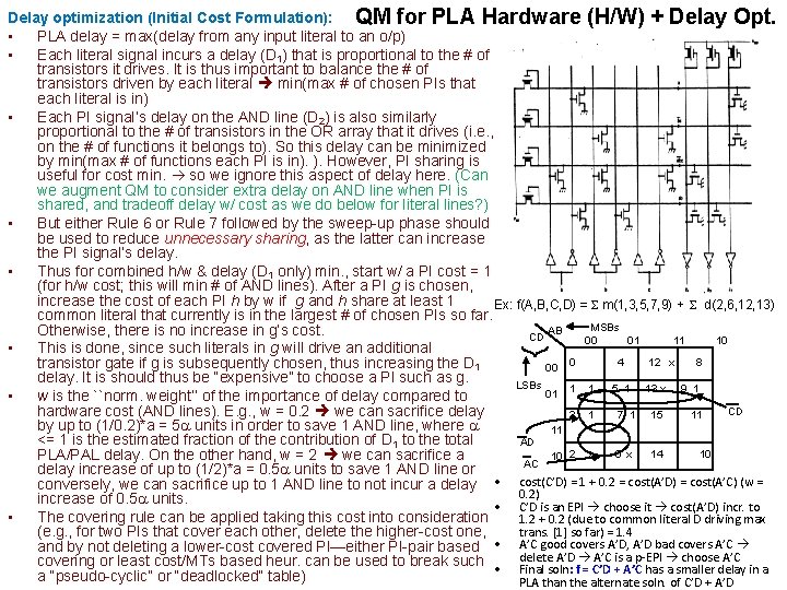
Delay optimization (Initial Cost Formulation): QM for PLA Hardware (H/W) + Delay Opt. • PLA delay = max(delay from any input literal to an o/p) • Each literal signal incurs a delay (D 1) that is proportional to the # of transistors it drives. It is thus important to balance the # of transistors driven by each literal min(max # of chosen PIs that each literal is in) • Each PI signal’s delay on the AND line (D 2) is also similarly proportional to the # of transistors in the OR array that it drives (i. e. , on the # of functions it belongs to). So this delay can be minimized by min(max # of functions each PI is in). ). However, PI sharing is useful for cost min. so we ignore this aspect of delay here. (Can we augment QM to consider extra delay on AND line when PI is shared, and tradeoff delay w/ cost as we do below for literal lines? ) • But either Rule 6 or Rule 7 followed by the sweep-up phase should be used to reduce unnecessary sharing, as the latter can increase the PI signal’s delay. • Thus for combined h/w & delay (D 1 only) min. , start w/ a PI cost = 1 (for h/w cost; this will min # of AND lines). After a PI g is chosen, increase the cost of each PI h by w if g and h share at least 1 Ex: f(A, B, C, D) = S m(1, 3, 5, 7, 9) + S d(2, 6, 12, 13) common literal that currently is in the largest # of chosen PIs so far. MSBs AB Otherwise, there is no increase in g’s cost. CD 00 01 11 10 • This is done, since such literals in g will drive an additional 4 12 x 8 transistor gate if g is subsequently chosen, thus increasing the D 1 00 0 delay. It is should thus be “expensive” to choose a PI such as g. LSBs 5 1 13 x 9 1 01 1 1 • w is the ``norm. weight’’ of the importance of delay compared to CD hardware cost (AND lines). E. g. , w = 0. 2 we can sacrifice delay 3 1 7 1 15 11 by up to (1/0. 2)*a = 5 a units in order to save 1 AND line, where a 11 <= 1 is the estimated fraction of the contribution of D 1 to the total AD 6 x 14 10 PLA/PAL delay. On the other hand, w = 2 we can sacrifice a 10 2 x AC delay increase of up to (1/2)*a = 0. 5 a units to save 1 AND line or conversely, we can sacrifice up to 1 AND line to not incur a delay • cost(C’D) = 1 + 0. 2 = cost(A’D) = cost(A’C) (w = 0. 2) increase of 0. 5 a units. • C’D is an EPI choose it cost(A’D) incr. to • The covering rule can be applied taking this cost into consideration 1. 2 + 0. 2 (due to common literal D driving max trans. [1] so far) = 1. 4 (e. g. , for two PIs that cover each other, delete the higher-cost one, • A’C good covers A’D, A’D bad covers A’C and by not deleting a lower-cost covered PI—either PI-pair based A’D A’C is a p-EPI choose A’C covering or least cost/MTs based heur. can be used to break such • delete Final soln: f = C’D + A’C has a smaller delay in a a “pseudo-cyclic” or “deadlocked” table) PLA than the alternate soln. of C’D + A’D

Delay optimization (Initial Cost Formulation): QM for PLA Hardware (H/W) + Delay Opt. • PLA delay = max(delay from any input literal to an o/p) • Each literal signal incurs a delay (D 1) that is proportional to the # of transistors it drives. It is thus important to balance the # of transistors driven by each literal min(max # of chosen PIs that each literal is in) • Each PI signal’s delay on the AND line (D 2) is also similarly proportional to the # of transistors in the OR array that it drives (i. e. , on the # of functions it belongs to). So this delay can be minimized by min(max # of functions each PI is in). However, PI sharing is useful for cost min. so we ignore this aspect of delay here. (Can we augment QM to consider extra delay on AND line when PI is shared, and tradeoff delay w/ cost as we do below for literal lines? ) • But either Rule 6 or Rule 7 followed by the sweep-up phase should be used to reduce unnecessary sharing, as the latter can increase the PI signal’s delay. • Thus for combined h/w & delay (D 1 only) min. , start w/ a PI cost = 1 (for h/w cost; this will min # of AND lines). After a PI g is chosen, Advanced Considerations—Not in Syllabus: increase the cost of each PI h by w if g and h share at least 1 • An alternate cost is to have the cost grow common literal that currently is in the largest # of chosen PIs so far. slowly as opposed to being binary w/ a sharp Otherwise, there is no increase in g’s cost. step (go from 0 to 1 as soon as a literal goes • This is done, since such literals in g will drive an additional from being in max-1 to max # of PIs so far). transistor gate if g is subsequently chosen, thus increasing the D 1 • So when PI g is selected, for every PI h that g delay. It is should thus be “expensive” to choose a PI such as g. has common literal(s) with, determine among • w is the ``norm. weight’’ of the importance of delay compared to these literals, the max. # k of chosen PIs they hardware cost (AND lines). E. g. , w = 0. 2 we can sacrifice delay occur in by up to (1/0. 2)*a = 5 a units in order to save 1 AND line, where a • E. g. , incr. cost by w*(e/(e-1))*(1 -e -(k/kmax) )) <= 1 is the estimated fraction of the contribution of D 1 to the total OR w(e-(1 -[k/kmax]) )) OR w*k/kmax, where kmax PLA/PAL delay. On the other hand, w = 2 we can sacrifice a is the globally max. # of chosen PIs that a delay increase of up to (1/2)*a = 0. 5 a units to save 1 AND line or literal (a critical literal) is currently present in. conversely, we can sacrifice up to 1 AND line to not incur a delay • This allows us to “anticipate” and consider increase of 0. 5 a units. costs of literals that can get critical in the near • The covering rule can be applied taking this cost into consideration future in the QM opt. process. (e. g. , for two PIs that cover each other, delete the higher-cost one, • But this does not do “look-ahead” (check and by not deleting a lower-cost covered PI—either PI-pair based what PIs are remaining and for each literal covering or least cost/MTs based heur. can be used to break such estimate how many it belongs to will be a “pseudo-cyclic” table) chosen. What is a good look-ahead estimate?