ECE 366 Computer Architecture Lecture 3 Shantanu Dutt
- Slides: 13

ECE 366 Computer Architecture Lecture 3 Shantanu Dutt (http: //www. ece. uic. edu/~dutt) Decomposition of Computer Organization & Generic Instruction Processing Note: These slides have been solely prepared by Shantanu Dutt. The “Patterson Fall 97 copyright UCB” logo appearing on the bottom right corner is incorrect (as is the logo on the bottom-left corner). They appear because the same template as Dave Patterson’s intro slides used in Lect. 1 -2 were used for these slides by mistake. The incorrect logos will be removed later (haven’t yet figured out how to). cs 152 L 1 Intro. 1 Patterson Fall 97 ©UCB

Overview ° Decomposition of a Computer ° Basic Functions of a Control Unit -- Read and Write Selects ° Generic Instruction Processing in the Control and Datapaths cs 152 L 1 Intro. 2 Patterson Fall 97 ©UCB

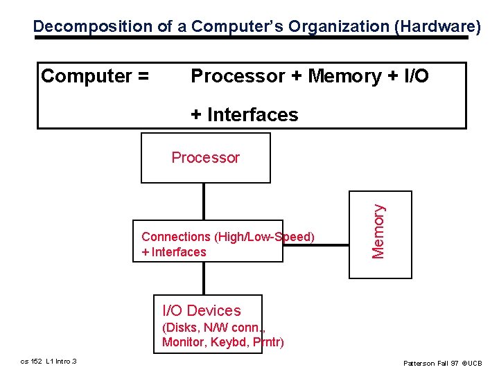
Decomposition of a Computer’s Organization (Hardware) Computer = Processor + Memory + I/O + Interfaces Connections (High/Low-Speed) + Interfaces Memory Processor I/O Devices (Disks, N/W conn. , Monitor, Keybd, Prntr) cs 152 L 1 Intro. 3 Patterson Fall 97 ©UCB

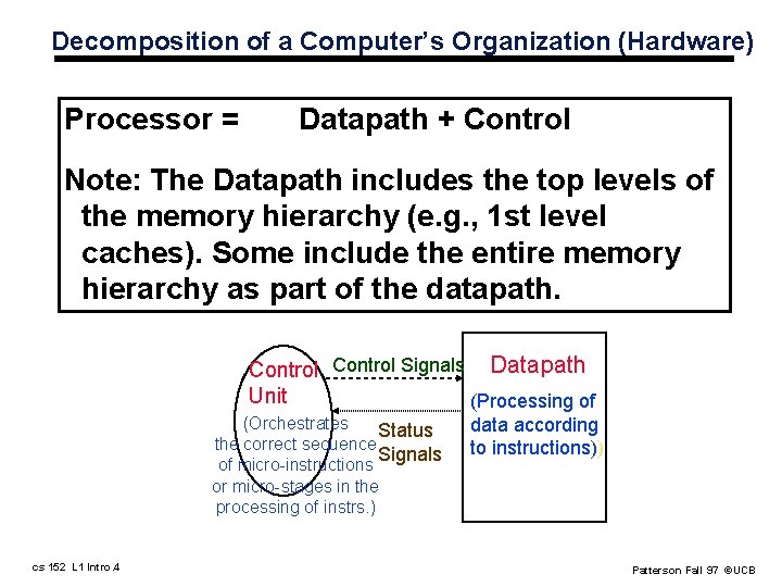
Decomposition of a Computer’s Organization (Hardware) Processor = Datapath + Control Note: The Datapath includes the top levels of the memory hierarchy (e. g. , 1 st level caches). Some include the entire memory hierarchy as part of the datapath. Control Signals Datapath Unit (Processing of (Orchestrates Status the correct sequence Signals of micro-instructions or micro-stages in the processing of instrs. ) cs 152 L 1 Intro. 4 data according to instructions)) Patterson Fall 97 ©UCB

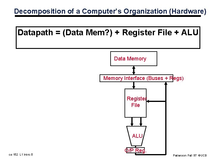
Decomposition of a Computer’s Organization (Hardware) Datapath = (Data Mem? ) + Register File + ALU Data Memory Interface (Buses + Regs) Register File ALU cs 152 L 1 Intro. 5 O/P Reg. Patterson Fall 97 ©UCB

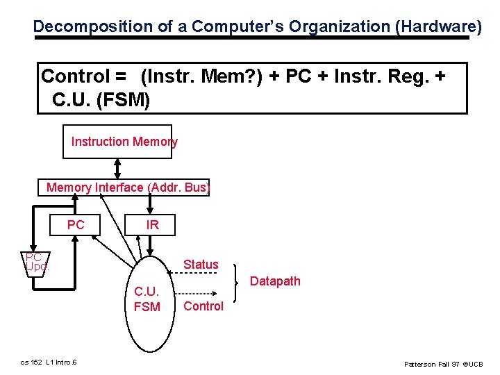
Decomposition of a Computer’s Organization (Hardware) Control = (Instr. Mem? ) + PC + Instr. Reg. + C. U. (FSM) Instruction Memory Interface (Addr. Bus) PC IR PC Upd. Status C. U. FSM cs 152 L 1 Intro. 6 Datapath Control Patterson Fall 97 ©UCB

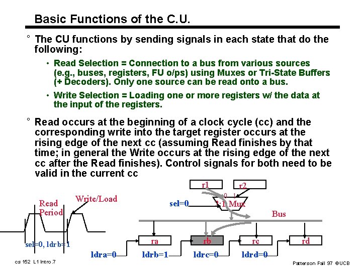
Basic Functions of the C. U. ° The CU functions by sending signals in each state that do the following: • Read Selection = Connection to a bus from various sources (e. g. , buses, registers, FU o/ps) using Muxes or Tri-State Buffers (+ Decoders). Only one source can be read onto a bus. • Write Selection = Loading one or more registers w/ the data at the input of the registers. ° Read occurs at the beginning of a clock cycle (cc) and the corresponding write into the target register occurs at the rising edge of the next cc (assuming Read finishes by that time; in general the Write occurs at the rising edge of the next cc after the Read finishes). Control signals for both need to be valid in the current cc r 1 Read Period Write/Load sel=0, ldrb=1 cs 152 L 1 Intro. 7 ldra=0 r 2 0 1 sel=0 2: 1 Mux Bus ra rb rc ldrb=1 ldrc=0 ldrd=0 rd Patterson Fall 97 ©UCB

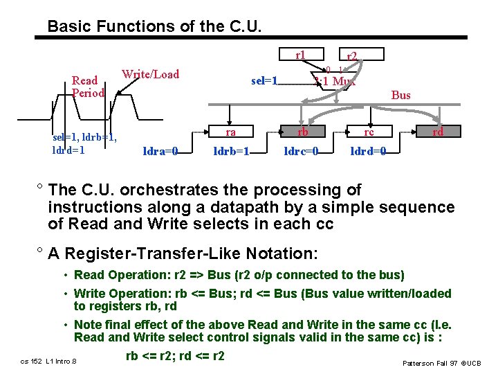
Basic Functions of the C. U. r 1 Read Period sel=1, ldrb=1, ldrd=1 Write/Load ldra=0 r 2 0 1 sel=1 2: 1 Mux Bus ra rb rc ldrb=1 ldrc=0 ldrd=0 rd ° The C. U. orchestrates the processing of instructions along a datapath by a simple sequence of Read and Write selects in each cc ° A Register-Transfer-Like Notation: • Read Operation: r 2 => Bus (r 2 o/p connected to the bus) • Write Operation: rb <= Bus; rd <= Bus (Bus value written/loaded to registers rb, rd • Note final effect of the above Read and Write in the same cc (I. e. Read and Write select control signals valid in the same cc) is : rb <= r 2; rd <= r 2 cs 152 L 1 Intro. 8 Patterson Fall 97 ©UCB

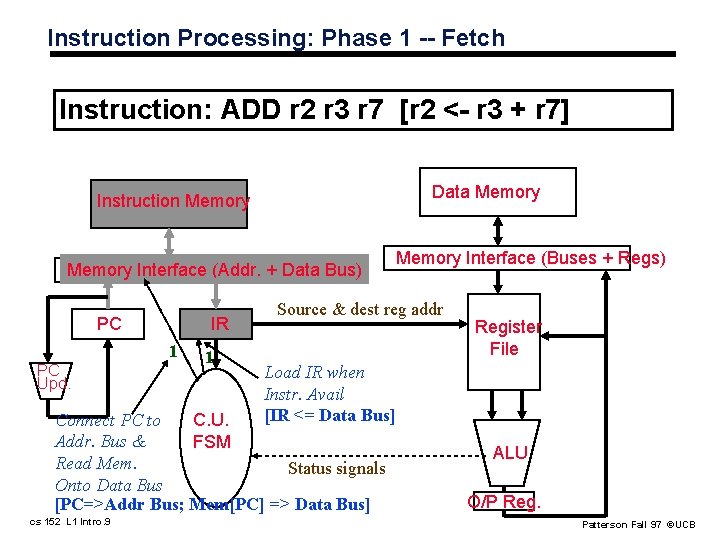
Instruction Processing: Phase 1 -- Fetch Instruction: ADD r 2 r 3 r 7 [r 2 <- r 3 + r 7] Data Memory Instruction Memory Interface (Addr. + Data Bus) PC IR 1 PC Upd. 1 Source & dest reg addr Register File Load IR when Instr. Avail [IR <= Data Bus] Connect PC to C. U. Addr. Bus & FSM Read Mem. Status signals Onto Data Bus [PC=>Addr Bus; Mem[PC] => Data Bus] cs 152 L 1 Intro. 9 Memory Interface (Buses + Regs) ALU O/P Reg. Patterson Fall 97 ©UCB

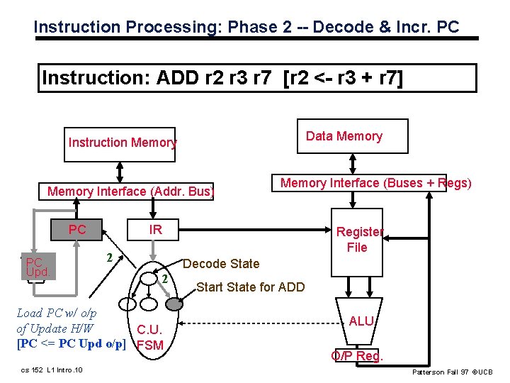
Instruction Processing: Phase 2 -- Decode & Incr. PC Instruction: ADD r 2 r 3 r 7 [r 2 <- r 3 + r 7] Data Memory Instruction Memory Interface (Addr. Bus) PC PC Upd. IR Register File 2 Decode State 2 Load PC w/ o/p of Update H/W C. U. [PC <= PC Upd o/p] FSM cs 152 L 1 Intro. 10 Memory Interface (Buses + Regs) Start State for ADD ALU O/P Reg. Patterson Fall 97 ©UCB

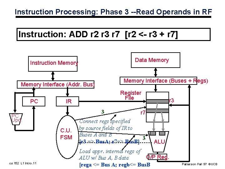
Instruction Processing: Phase 3 --Read Operands in RF Instruction: ADD r 2 r 3 r 7 [r 2 <- r 3 + r 7] Data Memory Instruction Memory Interface (Buses + Regs) Memory Interface (Addr. Bus) PC IR 3 PC Upd. C. U. FSM cs 152 L 1 Intro. 11 Register File r 3 r 7 Connect regs specified by source fields of IR to Buses A and B 3 [r 3 => Bus. A; r 7=> Bus. B] ALU Load appr. internal regs of O/P Reg. ALU w/ Bus A, B data [rega <= Bus A; regb<= Bus. B Patterson Fall 97 ©UCB

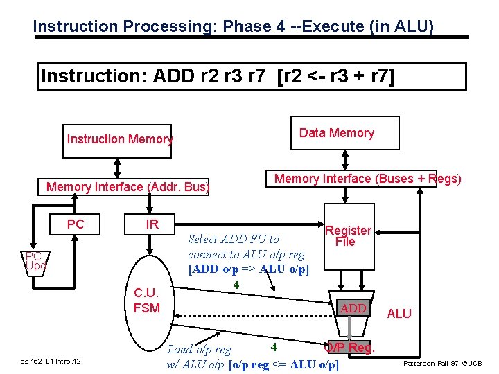
Instruction Processing: Phase 4 --Execute (in ALU) Instruction: ADD r 2 r 3 r 7 [r 2 <- r 3 + r 7] Data Memory Instruction Memory Interface (Addr. Bus) PC IR PC Upd. C. U. FSM cs 152 L 1 Intro. 12 Memory Interface (Buses + Regs) Select ADD FU to connect to ALU o/p reg [ADD o/p => ALU o/p] 4 Register File ADD 4 O/P Reg. Load o/p reg w/ ALU o/p [o/p reg <= ALU o/p] ALU Patterson Fall 97 ©UCB

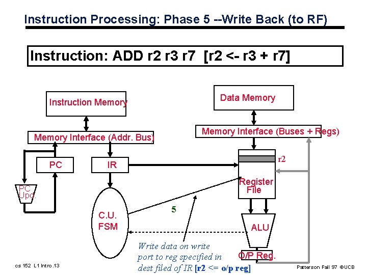
Instruction Processing: Phase 5 --Write Back (to RF) Instruction: ADD r 2 r 3 r 7 [r 2 <- r 3 + r 7] Data Memory Instruction Memory Interface (Buses + Regs) Memory Interface (Addr. Bus) PC r 2 IR Register File PC Upd. C. U. FSM cs 152 L 1 Intro. 13 5 ALU Write data on write O/P Reg. port to reg specified in dest filed of IR [r 2 <= o/p reg] Patterson Fall 97 ©UCB