Numerical Technologies Inc 4 13 99 Tutorial on


- Slides: 29
Numerical Technologies, Inc 4 -13 -99 Tutorial on Subwavelength Lithography DAC 99 Y. C. (Buno) Pati Numerical Technologies, Inc.
DAC 99 June 24, 1999 Agenda n Background n The Sub. Wavelength Gap n Sub. Wavelength Technologies ¨ ¨ Optical proximity correction (OPC) Phase shifting Process modeling Silicon Level Verification n Some implications for physical design? 4 -13 -99
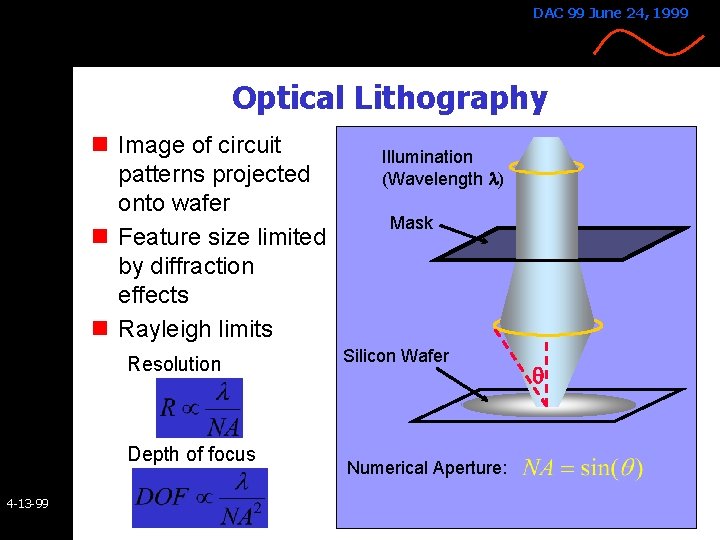
DAC 99 June 24, 1999 Optical Lithography n Image of circuit patterns projected onto wafer n Feature size limited by diffraction effects n Rayleigh limits Resolution Depth of focus 4 -13 -99 Illumination (Wavelength l) Mask Silicon Wafer Numerical Aperture: q
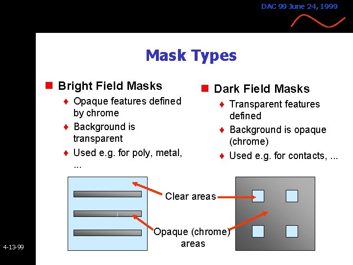
DAC 99 June 24, 1999 Mask Types n Bright Field Masks ¨ Opaque features defined by chrome ¨ Background is transparent ¨ Used e. g. for poly, metal, . . . n Dark Field Masks ¨ Transparent features defined ¨ Background is opaque (chrome) ¨ Used e. g. for contacts, . . . Clear areas 4 -13 -99 Opaque (chrome) areas
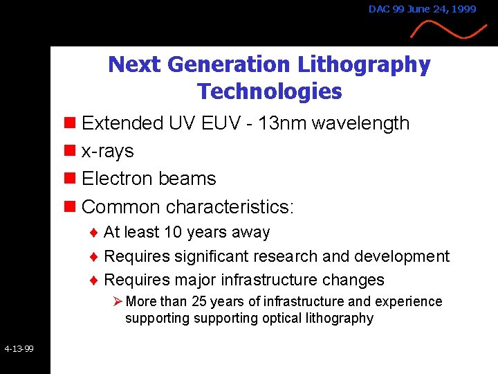
DAC 99 June 24, 1999 Next Generation Lithography Technologies n Extended UV EUV - 13 nm wavelength n x-rays n Electron beams n Common characteristics: ¨ At least 10 years away ¨ Requires significant research and development ¨ Requires major infrastructure changes Ø More than 25 years of infrastructure and experience supporting optical lithography 4 -13 -99
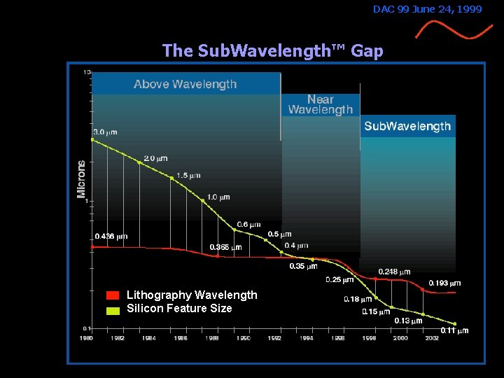
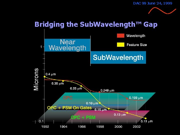
DAC 99 June 24, 1999 The Sub. Wavelength™ Gap Lithography Wavelength Silicon Feature Size 4 -13 -99
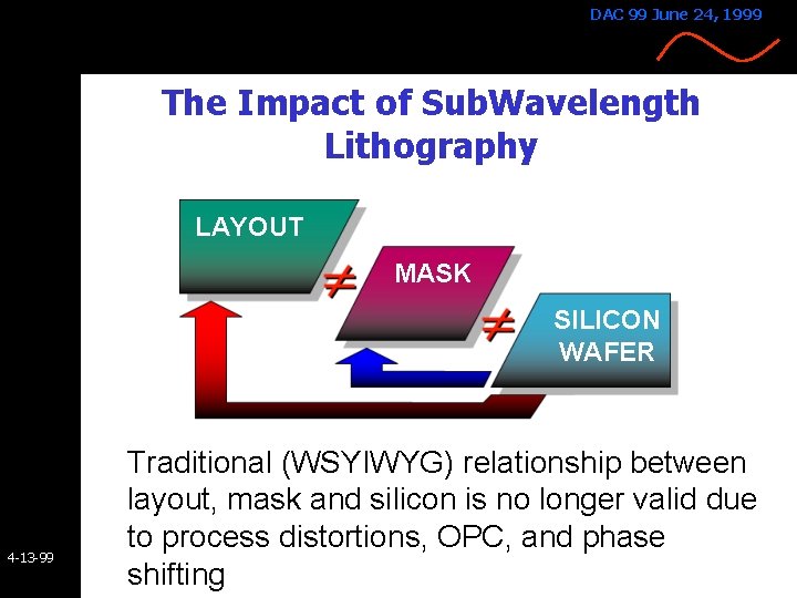
DAC 99 June 24, 1999 The Impact of Sub. Wavelength Lithography LAYOUT MASK SILICON WAFER 4 -13 -99 Traditional (WSYIWYG) relationship between layout, mask and silicon is no longer valid due to process distortions, OPC, and phase shifting
DAC 99 June 24, 1999 Bridging the Sub. Wavelength™ Gap 4 -13 -99
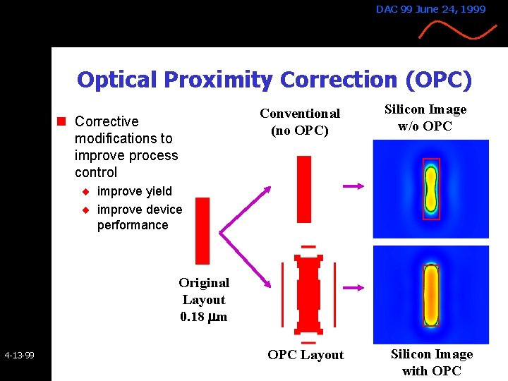
DAC 99 June 24, 1999 Optical Proximity Correction (OPC) Conventional (no OPC) n Corrective modifications to improve process control Silicon Image w/o OPC ¨ improve yield ¨ improve device performance Original Layout 0. 18 mm 4 -13 -99 OPC Layout Silicon Image with OPC
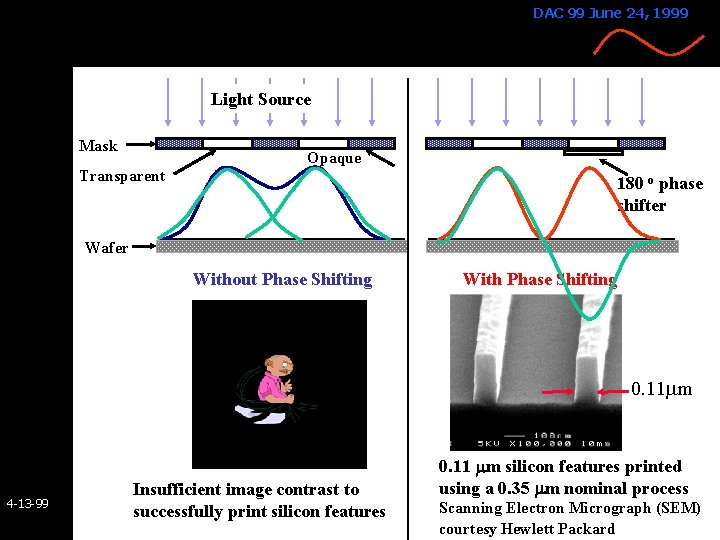
DAC 99 June 24, 1999 Phase-Shifting (PSM) Technology n Phase modulation used at mask level to Gate lengths reduced to 0. 1 mm Silicon Image w/o PSM Layout Silicon Image with PSM ¨ reduce feature size ¨ improve yield ¨ improve device performance 4 -13 -99 Original Layout 0. 18 mm
DAC 99 June 24, 1999 Light Source Mask Opaque Transparent 180 o phase shifter Wafer Without Phase Shifting With Phase Shifting 0. 11 mm 4 -13 -99 Insufficient image contrast to successfully print silicon features 0. 11 mm silicon features printed using a 0. 35 mm nominal process Scanning Electron Micrograph (SEM) courtesy Hewlett Packard
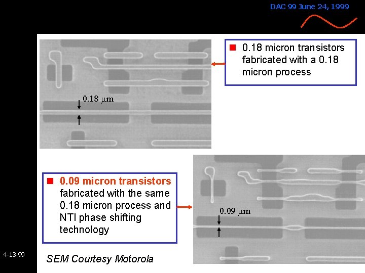
DAC 99 June 24, 1999 n 0. 18 micron transistors fabricated with a 0. 18 micron process 0. 18 mm n 0. 09 micron transistors fabricated with the same 0. 18 micron process and NTI phase shifting technology 4 -13 -99 SEM Courtesy Motorola 0. 09 mm
DAC 99 June 24, 1999 Optical Proximity Correction n Goal: Improve device performance and yield ¨ Cosmetic correction complicates mask manufacturing and dramatically increases cost with little benefit n OPC is not new, it’s just more complicated than it was before n Key issues: 4 -13 -99 ¨ Manufacturability ¨ Design and verification tools OPC Features ¨ Serifs - for corner rounding ¨ Hammerheads - for line-end shortening ¨ Assists - for CD control ¨ Biasing - for CD control
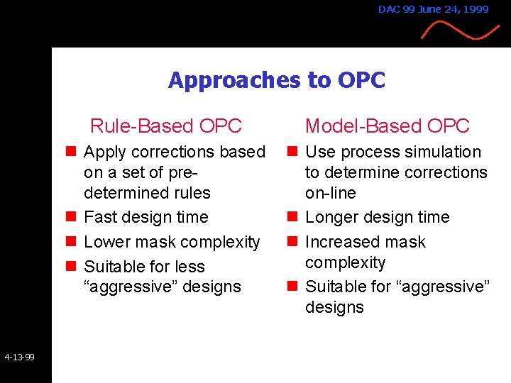
DAC 99 June 24, 1999 Approaches to OPC 4 -13 -99 Rule-Based OPC Model-Based OPC n Apply corrections based on a set of predetermined rules n Fast design time n Lower mask complexity n Suitable for less “aggressive” designs n Use process simulation to determine corrections on-line n Longer design time n Increased mask complexity n Suitable for “aggressive” designs
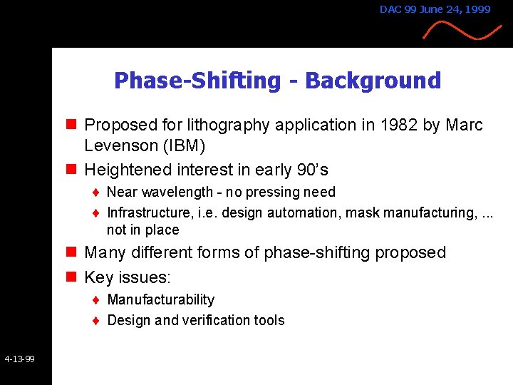
DAC 99 June 24, 1999 Phase-Shifting - Background n Proposed for lithography application in 1982 by Marc Levenson (IBM) n Heightened interest in early 90’s ¨ Near wavelength - no pressing need ¨ Infrastructure, i. e. design automation, mask manufacturing, . . . not in place n Many different forms of phase-shifting proposed n Key issues: ¨ Manufacturability ¨ Design and verification tools 4 -13 -99
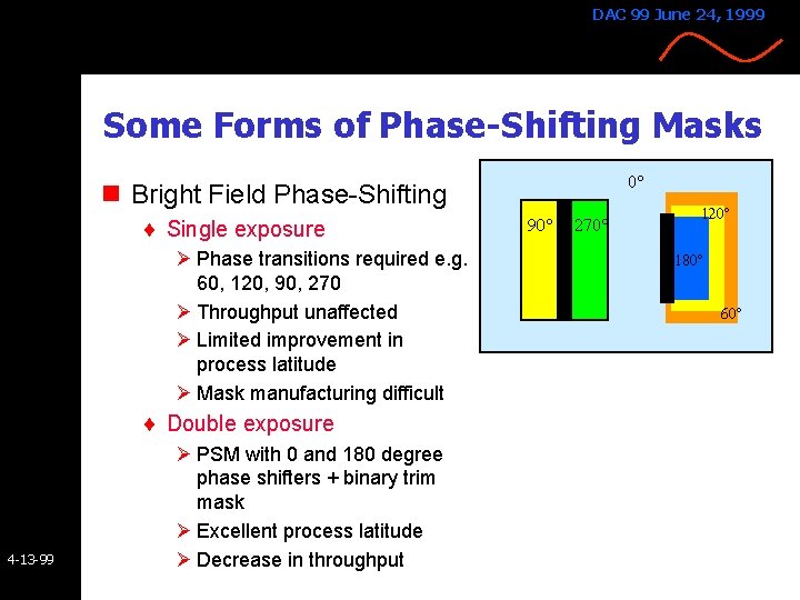
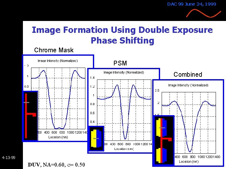
DAC 99 June 24, 1999 Some Forms of Phase-Shifting Masks 0 n Bright Field Phase-Shifting ¨ Single exposure Ø Phase transitions required e. g. 60, 120, 90, 270 Ø Throughput unaffected Ø Limited improvement in process latitude Ø Mask manufacturing difficult ¨ Double exposure 4 -13 -99 Ø PSM with 0 and 180 degree phase shifters + binary trim mask Ø Excellent process latitude Ø Decrease in throughput 90 270 120 180 60
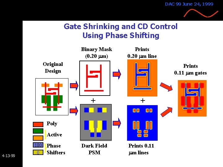
DAC 99 June 24, 1999 Gate Shrinking and CD Control Using Phase Shifting Binary Mask (0. 20 mm) Prints 0. 20 mm line Original Design Prints 0. 11 mm gates + + Dark Field PSM Prints 0. 11 mm lines Poly Active 4 -13 -99 180 0 Phase Shifters
DAC 99 June 24, 1999 Image Formation Using Double Exposure Phase Shifting Chrome Mask PSM Combined 4 -13 -99 DUV, NA=0. 60, s= 0. 50
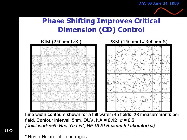
DAC 99 June 24, 1999 Phase Shifting Improves Critical Dimension (CD) Control BIM (250 nm L/S ) PSM (150 nm L/ 300 nm S) Line width contours shown for a full wafer (45 fields, 36 measurements per field. Contour interval: 5 nm. DUV, NA = 0. 42, s = 0. 5 (Joint work with Hua-Yu Liu*, HP ULSI Research Laboratories) 4 -13 -99 * Now at Numerical Technologies
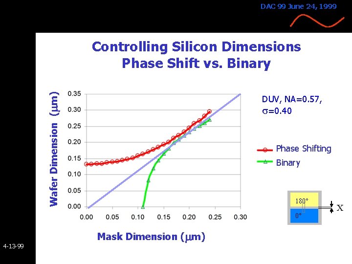
DAC 99 June 24, 1999 Wafer Dimension (mm) Controlling Silicon Dimensions Phase Shift vs. Binary DUV, NA=0. 57, s=0. 40 Phase Shifting Binary 180° 0° 4 -13 -99 Mask Dimension (mm) X
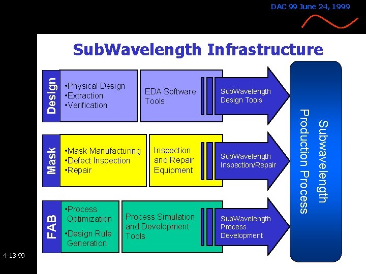
DAC 99 June 24, 1999 Design FAB 4 -13 -99 • Process Optimization • Design Rule Generation Inspection and Repair Equipment Process Simulation and Development Tools Sub. Wavelength Design Tools Sub. Wavelength Inspection/Repair Sub. Wavelength Process Development Subwavelength • Mask Manufacturing • Defect Inspection • Repair EDA Software Tools Production Process • Physical Design • Extraction • Verification Mask Sub. Wavelength Infrastructure
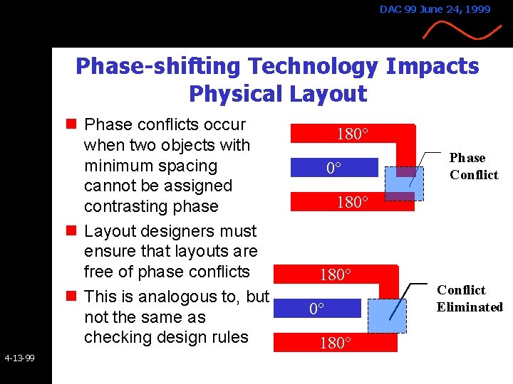
DAC 99 June 24, 1999 Phase-shifting Technology Impacts Physical Layout n Phase conflicts occur when two objects with minimum spacing cannot be assigned contrasting phase n Layout designers must ensure that layouts are free of phase conflicts n This is analogous to, but not the same as checking design rules 4 -13 -99 180° 0° Phase Conflict 180° 0° 180° Conflict Eliminated
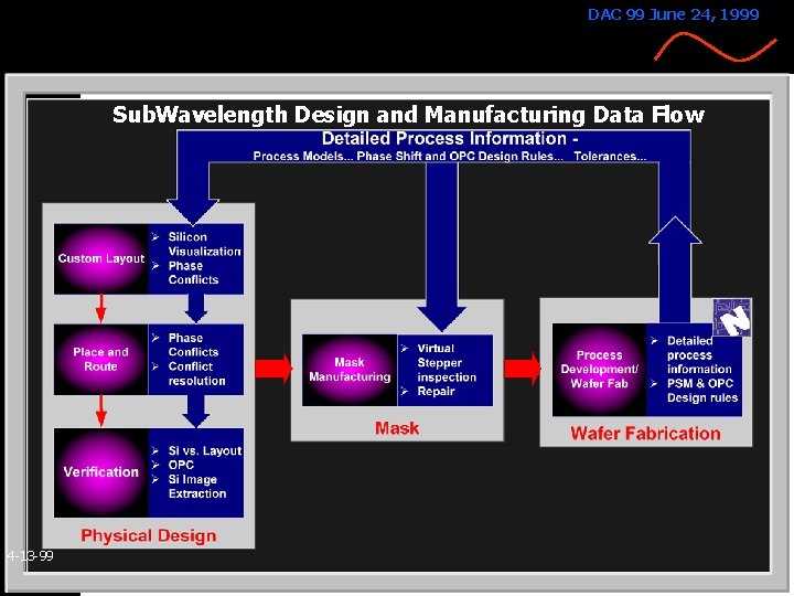
DAC 99 June 24, 1999 Sub. Wavelength Design and Manufacturing Data Flow 4 -13 -99
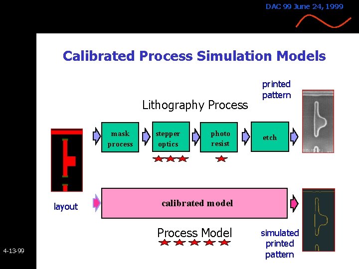
DAC 99 June 24, 1999 Calibrated Process Simulation Models Lithography Process mask process layout stepper optics photo resist etch calibrated model Process Model 4 -13 -99 printed pattern simulated printed pattern
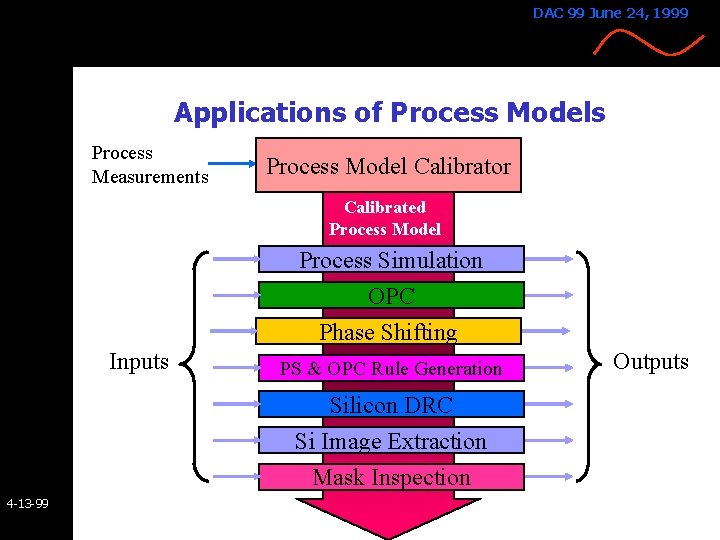
DAC 99 June 24, 1999 Applications of Process Models Process Measurements Process Model Calibrator Calibrated Process Model Process Simulation OPC Phase Shifting Inputs PS & OPC Rule Generation Silicon DRC Si Image Extraction Mask Inspection 4 -13 -99 Outputs
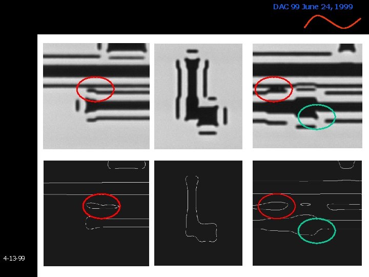
DAC 99 June 24, 1999 4 -13 -99
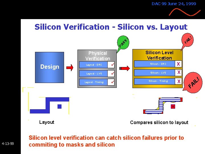
DAC 99 June 24, 1999 PA SS FA ! IL ! Silicon Verification - Silicon vs. Layout 4 -13 -99 ü Silicon - DRC X Layout - LVS ü Silicon - LVS X Layout - Timing ü Silicon - Timing X FA IL Design Layout - DRC ! Silicon Level Verification Physical Verification Compares silicon to layout Silicon level verification catch silicon failures prior to commiting to masks and silicon
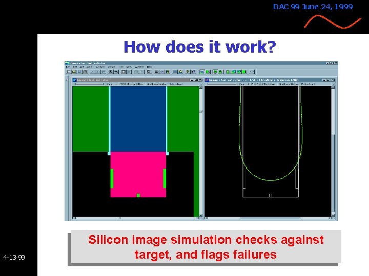
DAC 99 June 24, 1999 How does it work? 4 -13 -99 Silicon image simulation checks against target, and flags failures
DAC 99 June 24, 1999 Summary n Sub. Wavelength technologies are critical to IC manufacturing for the next 7 -10 years ¨ OPC is a corrective technology ¨ Phase shifting is an enabling technology n Sub. Wavelength design and manufacturing requires the coordinated interaction of physical design with lithography process, semiconductor equipment, and mask manufacturing n Moore’s Law will live on (for now)! …. 4 -13 -99