Monolith IC 3 D ICs RCAT approach Monolith
- Slides: 29
Monolith. IC 3 D ICs RCAT approach Monolith. IC 3 D Inc. , Patents Pending 1
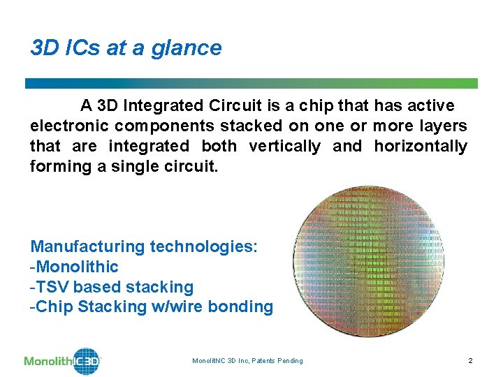
3 D ICs at a glance A 3 D Integrated Circuit is a chip that has active electronic components stacked on one or more layers that are integrated both vertically and horizontally forming a single circuit. Manufacturing technologies: -Monolithic -TSV based stacking -Chip Stacking w/wire bonding Monolith. IC 3 D Inc, Patents Pending 2
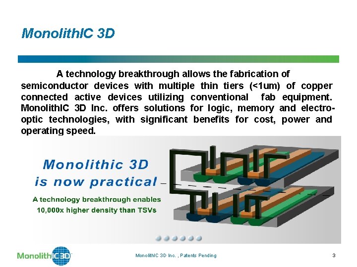
Monolith. IC 3 D A technology breakthrough allows the fabrication of semiconductor devices with multiple thin tiers (<1 um) of copper connected active devices utilizing conventional fab equipment. Monolith. IC 3 D Inc. offers solutions for logic, memory and electrooptic technologies, with significant benefits for cost, power and operating speed. Monolith. IC 3 D Inc. , Patents Pending 3
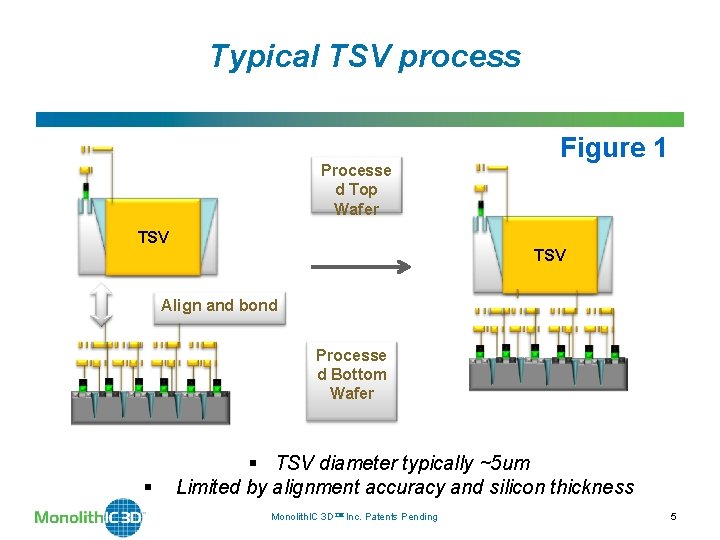
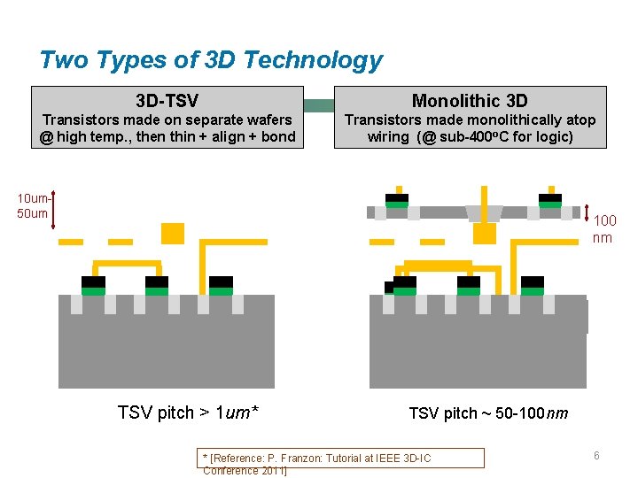
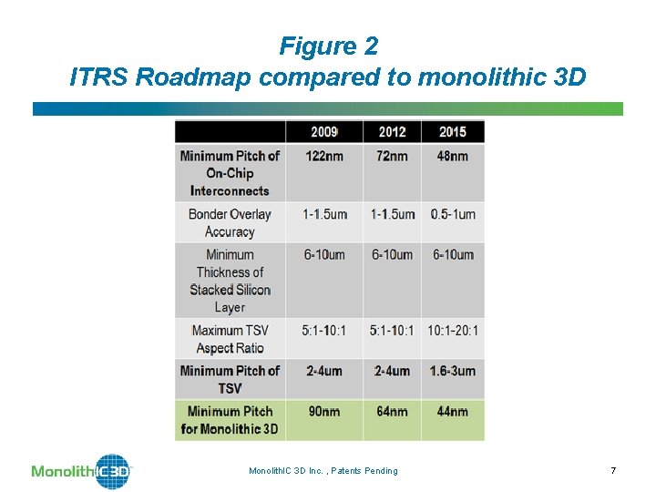
Comparison of Through-Silicon Via (TSV) 3 D Technology and Monolithic 3 D Technology The semiconductor industry is actively pursuing 3 D Integrated Circuits (3 D-ICs) with Through-Silicon Via (TSV) technology (Figure 1). This can also be called a parallel 3 D process. As shown in Figure 2, the International Technology Roadmap for Semiconductors (ITRS) projects TSV pitch remaining in the range of several microns, while on-chip interconnect pitch is in the range of 100 nm. The TSV pitch will not reduce appreciably in the future due to bonder alignment limitations (0. 5 -1 um) and stacked silicon layer thickness (6 -10 um). While the micron-ranged TSV pitches may provide enough vertical connections for stacking memory atop processors and memory-on-memory stacking, they may not be enough to significantly mitigate the well-known onchip interconnect problems. Monolithic 3 D-ICs offer through-silicon connections with <50 nm diameter and therefore provide 10, 000 times the areal density of TSV technology. Monolith. IC 3 D Inc. , Patents Pending 4
Typical TSV process Processe d Top Wafer Figure 1 TSV Align and bond Processe d Bottom Wafer § TSV diameter typically ~5 um § Limited by alignment accuracy and silicon thickness Monolith. IC 3 D Inc. Patents Pending 5
Two Types of 3 D Technology 3 D-TSV Monolithic 3 D Transistors made on separate wafers @ high temp. , then thin + align + bond Transistors made monolithically atop wiring (@ sub-400 o. C for logic) 10 um 50 um 100 nm TSV pitch > 1 um* TSV pitch ~ 50 -100 nm * [Reference: P. Franzon: Tutorial at IEEE 3 D-IC Conference 2011] 6
Figure 2 ITRS Roadmap compared to monolithic 3 D Monolith. IC 3 D Inc. , Patents Pending 7
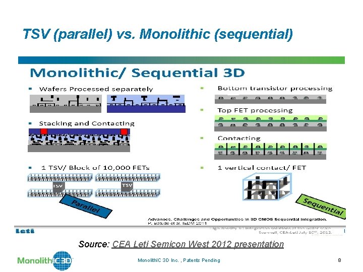
TSV (parallel) vs. Monolithic (sequential) Source: CEA Leti Semicon West 2012 presentation Monolith. IC 3 D Inc. , Patents Pending 8
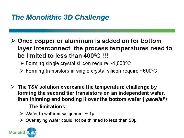
The Monolithic 3 D Challenge Ø Once copper or aluminum is added on for bottom layer interconnect, the process temperatures need to be limited to less than 400ºC !!! Ø Forming single crystal silicon require ~1, 000ºC Ø Forming transistors in single crystal silicon require ~800ºC Ø The TSV solution overcame the temperature challenge by forming the second tier transistors on an independent wafer, then thinning and bonding it over the bottom wafer (‘parallel’) The limitations: Ø Wafer to wafer misalignment ~ 1µ Ø Overlaying wafer could not be thinned to less than 50µ
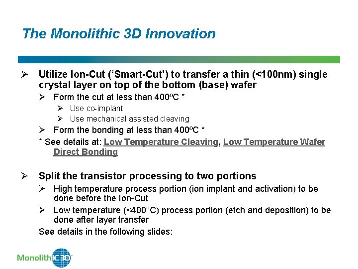
The Monolithic 3 D Innovation Ø Utilize Ion-Cut (‘Smart-Cut’) to transfer a thin (<100 nm) single crystal layer on top of the bottom (base) wafer Ø Form the cut at less than 400ºC * Ø Use co-implant Ø Use mechanical assisted cleaving Ø Form the bonding at less than 400ºC * * See details at: Low Temperature Cleaving, Low Temperature Wafer Direct Bonding Ø Split the transistor processing to two portions Ø High temperature process portion (ion implant and activation) to be done before the Ion-Cut Ø Low temperature (<400°C) process portion (etch and deposition) to be done after layer transfer See details in the following slides:
Monolithic 3 D ICs Using Smart. Cut technology - the ion cutting process that Soitec uses to make SOI wafers for AMD and IBM (million of wafers had utilized the process over the last 20 years) - to stack up consecutive layers of active silicon (bond first and then cut). Soitec’s Smart Cut Patented* Flow: *Soitec’s fundamental patent US 5, 374, 564 expired Sep. 15, 2012 Monolith. IC 3 D Inc. , Patents Pending 11
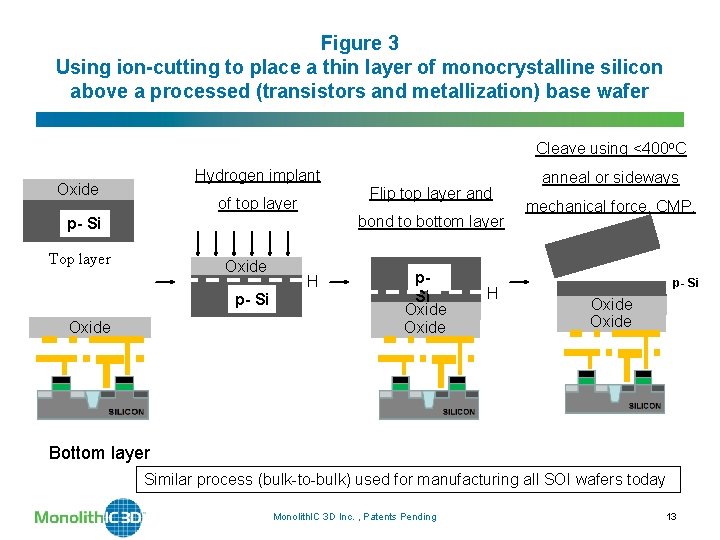
Monolithic 3 D ICs Ion cutting: the key idea is that if you implant a thin layer of H+ ions into a single crystal of silicon, the ions will weaken the bonds between the neighboring silicon atoms, creating a fracture plane (Figure 3). Judicious force will then precisely break the wafer at the plane of the H+ implant, allowing you to in effect peel off very thin layer. This technique is currently being used to produce the most advanced transistors (Fully Depleted SOI, UTBB transistors – Ultra Thin Body and BOX), forming monocrystalline silicon layers that are less than 10 nm thick. Monolith. IC 3 D Inc. , Patents Pending 12
Figure 3 Using ion-cutting to place a thin layer of monocrystalline silicon above a processed (transistors and metallization) base wafer Cleave using <400 o. C Hydrogen implant Oxide Flip top layer and of top layer bond to bottom layer p- Si Top layer Oxide p- Si Oxide H p. Si Oxide H anneal or sideways mechanical force. CMP. p- Si Oxide Bottom layer Similar process (bulk-to-bulk) used for manufacturing all SOI wafers today Monolith. IC 3 D Inc. , Patents Pending 13
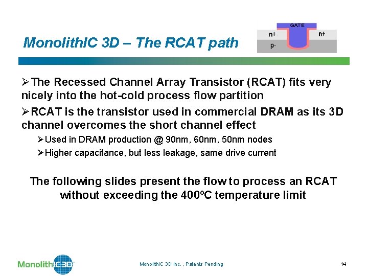
Monolith. IC 3 D – The RCAT path ØThe Recessed Channel Array Transistor (RCAT) fits very nicely into the hot-cold process flow partition ØRCAT is the transistor used in commercial DRAM as its 3 D channel overcomes the short channel effect ØUsed in DRAM production @ 90 nm, 60 nm, 50 nm nodes ØHigher capacitance, but less leakage, same drive current The following slides present the flow to process an RCAT without exceeding the 400ºC temperature limit Monolith. IC 3 D Inc. , Patents Pending 14
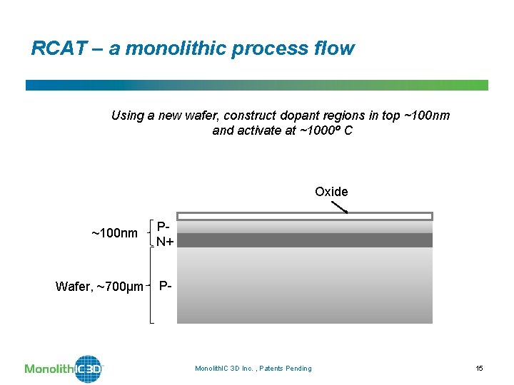
RCAT – a monolithic process flow Using a new wafer, construct dopant regions in top ~100 nm and activate at ~1000º C Oxide ~100 nm Wafer, ~700µm PN+ P- Monolith. IC 3 D Inc. , Patents Pending 15
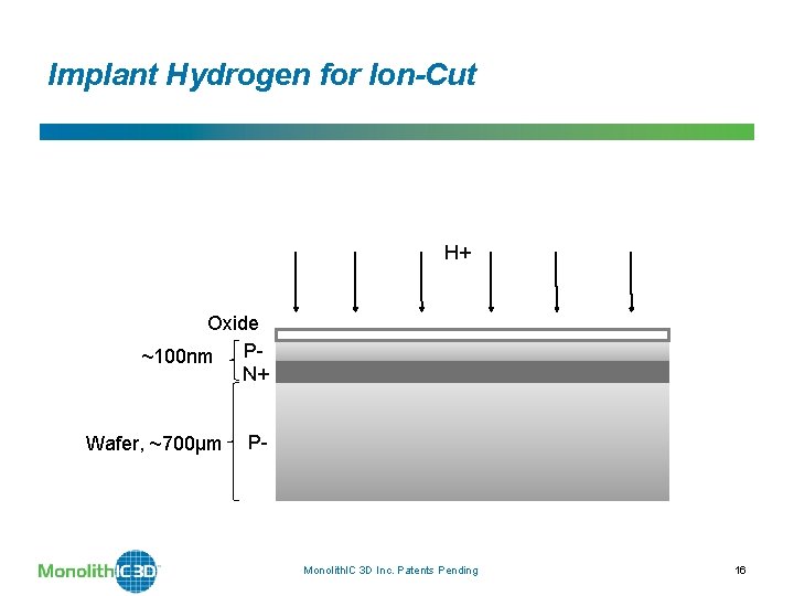
Implant Hydrogen for Ion-Cut H+ Oxide P~100 nm N+ Wafer, ~700µm P- Monolith. IC 3 D Inc. Patents Pending 16
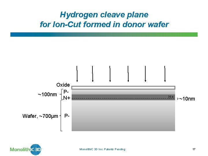
Hydrogen cleave plane for Ion-Cut formed in donor wafer Oxide P~100 nm N+ Wafer, ~700µm H+ ~10 nm P- Monolith. IC 3 D Inc. Patents Pending 17
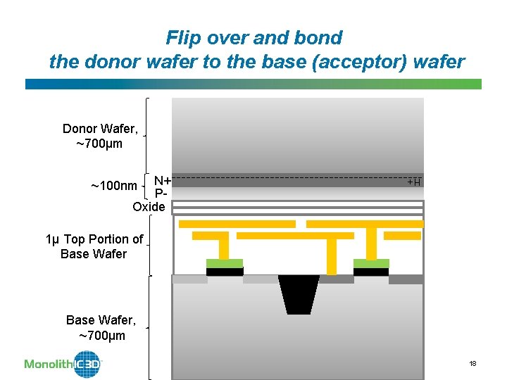
Flip over and bond the donor wafer to the base (acceptor) wafer Donor Wafer, ~700µm N+ POxide H+ ~100 nm 1µ Top Portion of Base Wafer, ~700µm Monolith. IC 3 D Inc. Patents Pending 18
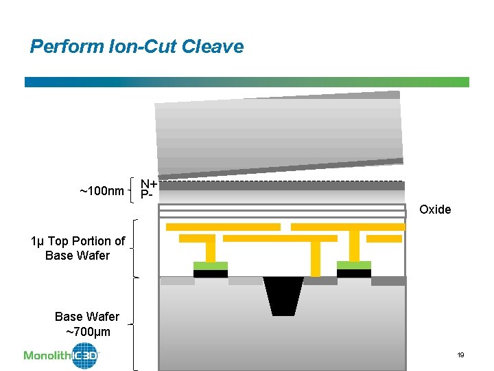
Perform Ion-Cut Cleave ~100 nm N+ POxide 1µ Top Portion of Base Wafer Monolith. IC 3 D Inc. Patents Pending Base Wafer ~700µm 19
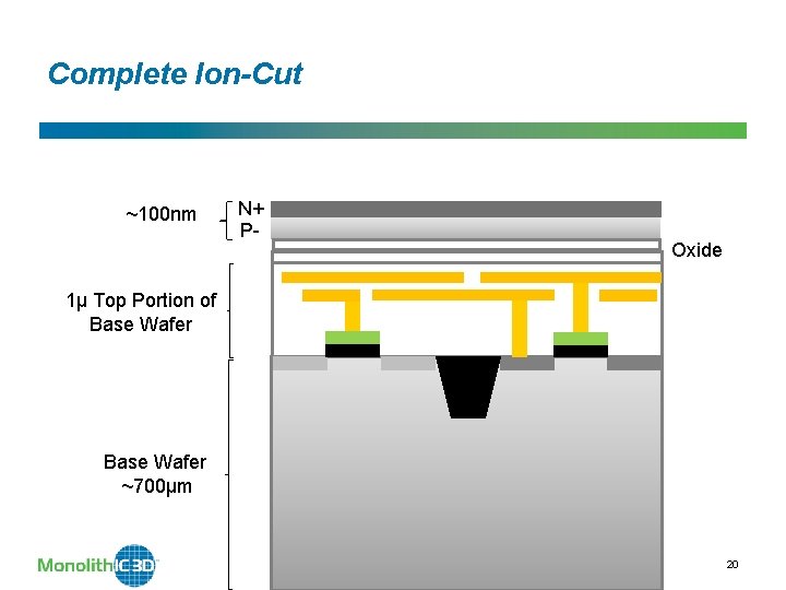
Complete Ion-Cut ~100 nm N+ P- Oxide 1µ Top Portion of Base Wafer Monolith. IC 3 D Inc. Patents Pending Base Wafer ~700µm 20
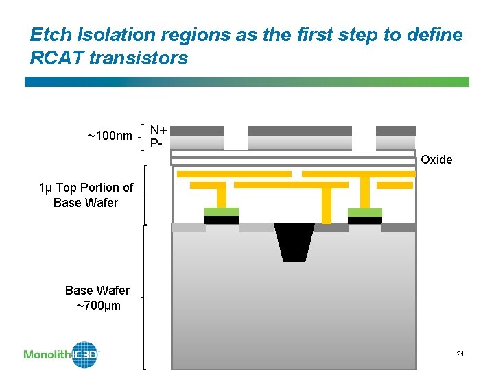
Etch Isolation regions as the first step to define RCAT transistors ~100 nm N+ POxide 1µ Top Portion of Base Wafer Monolith. IC 3 D Inc. Patents Pending Base Wafer ~700µm 21
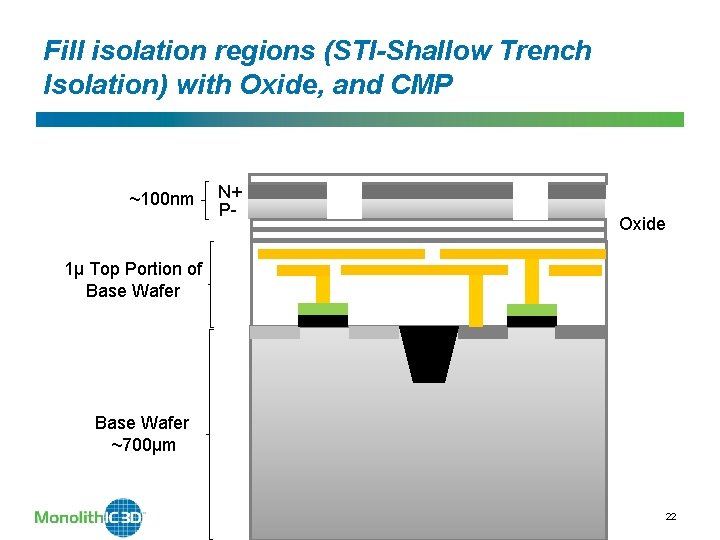
Fill isolation regions (STI-Shallow Trench Isolation) with Oxide, and CMP ~100 nm N+ P- Oxide 1µ Top Portion of Base Wafer Monolith. IC 3 D Inc. Patents Pending Base Wafer ~700µm 22
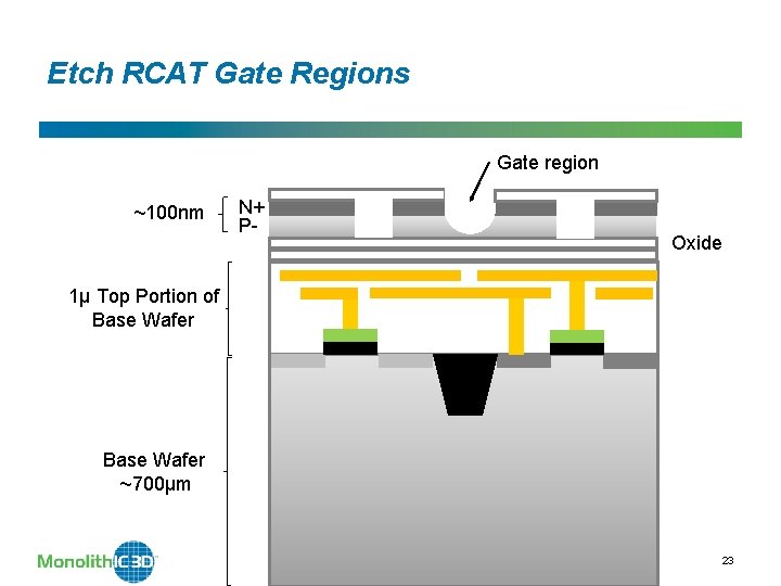
Etch RCAT Gate Regions Gate region ~100 nm N+ P- Oxide 1µ Top Portion of Base Wafer Monolith. IC 3 D Inc. Patents Pending Base Wafer ~700µm 23
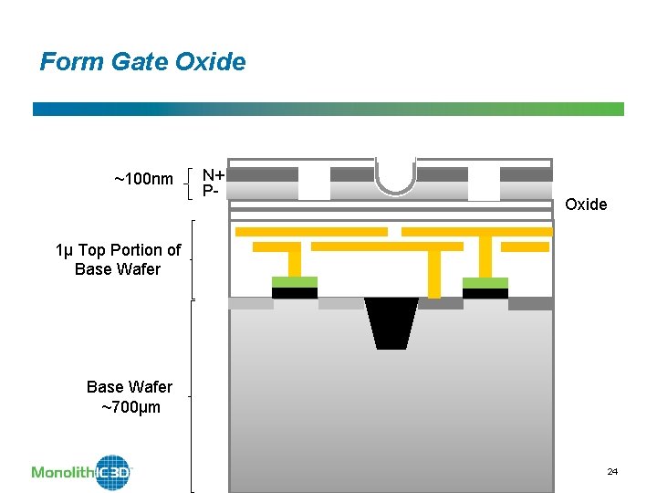
Form Gate Oxide ~100 nm N+ P- Oxide 1µ Top Portion of Base Wafer Monolith. IC 3 D Inc. Patents Pending Base Wafer ~700µm 24
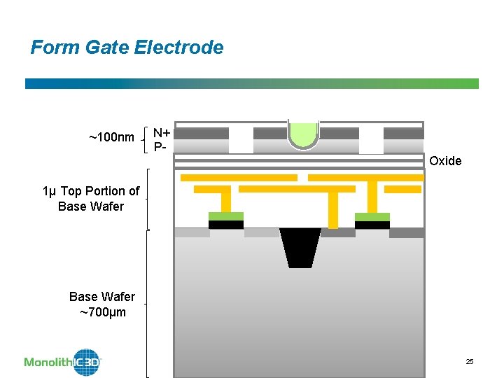
Form Gate Electrode ~100 nm N+ POxide 1µ Top Portion of Base Wafer Monolith. IC 3 D Inc. Patents Pending Base Wafer ~700µm 25
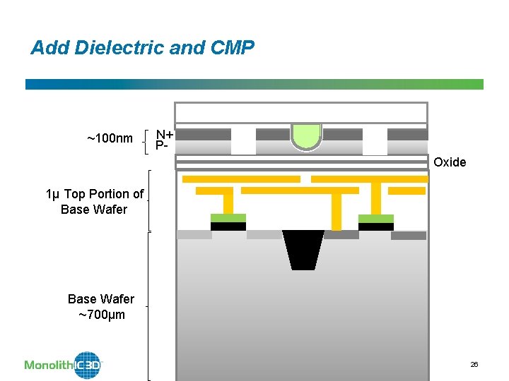
Add Dielectric and CMP ~100 nm N+ POxide 1µ Top Portion of Base Wafer Monolith. IC 3 D Inc. Patents Pending Base Wafer ~700µm 26
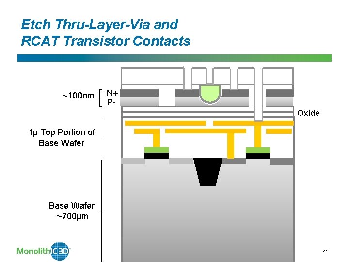
Etch Thru-Layer-Via and RCAT Transistor Contacts ~100 nm N+ POxide 1µ Top Portion of Base Wafer Monolith. IC 3 D Inc. Patents Pending Base Wafer ~700µm 27
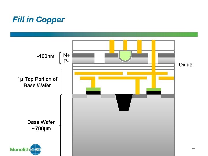
Fill in Copper ~100 nm N+ P- Oxide 1µ Top Portion of Base Wafer Monolith. IC 3 D Inc. Patents Pending Base Wafer ~700µm 28
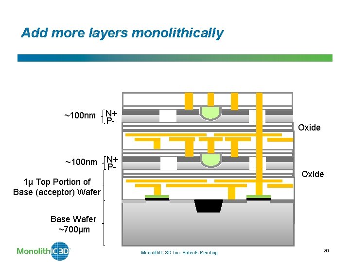
Add more layers monolithically ~100 nm N+ P- Oxide 1µ Top Portion of Base (acceptor) Wafer Base Wafer ~700µm Monolith. IC 3 D Inc. Patents Pending 29