Layout of the ITk Pixel Detector New layout
- Slides: 6

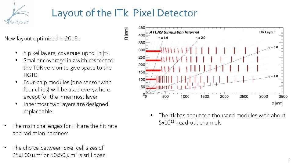
Layout of the ITk Pixel Detector New layout optimized in 2018 : • 5 pixel layers, coverage up to |h|=4 • Smaller coverage in z with respect to the TDR version to give space to the HGTD • Four-chip modules (one sensor with four chips) will be used everywhere, except for the innermost layer • Innermost two layers are designed replaceable • The main challenges for ITk are the hit rate and radiation hardness • The choice between pixel cell sizes of 25 x 100 mm 2 or 50 x 50 mm 2 is still open • The Itk has about ten thousand modules with about 5 x 10¹⁹ read-out channels 1

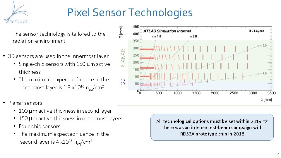
Pixel Sensor Technologies 3 D • 3 D sensors are used in the innermost layer • Single-chip sensors with 150 mm active thickness • The maximum expected fluence in the innermost layer is 1. 3 x 10¹⁶ neq/cm 2 PLANAR The sensor technology is tailored to the radiation environment • Planar sensors • 100 mm active thickness in second layer • 150 mm active thickness in outermost layers • Four-chip sensors • The maximum expected fluence in the second layer is 4 x 10¹⁵ neq/cm 2 All technological options must be set within 2019 There was an intense test-beam campaign with RD 53 A prototype chip in 2018 2

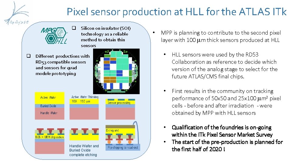
Pixel sensor production at HLL for the ATLAS ITk q Silicon on insulator (SOI) technology as a reliable method to obtain thin sensors q Different productions with RD 53 compatible sensors and sensors for quad module prototyping • MPP is planning to contribute to the second pixel layer with 100 mm thick sensors produced at HLL • HLL sensors were used by the RD 53 Collaboration as reference to decide which version of the analog stage to select for the future ATLAS/CMS final chips. • First results in the community on tracking performance of 50 x 50 and 25 x 100 mm 2 pixel cells - before and after irradiation - were obtained by MPP with HLL sensors Handle Wafer and Buried Oxide complete etching • Qualification of the foundries is on-going within the ITk Pixel Sensor Market Survey • The start of the pre-production is planned for the first half of 2020 !

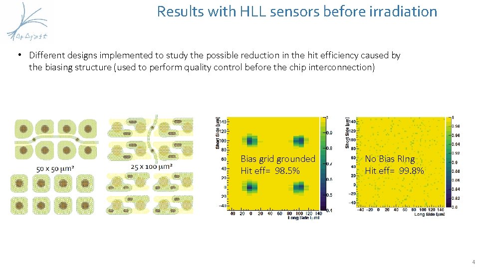
Results with HLL sensors before irradiation • Different designs implemented to study the possible reduction in the hit efficiency caused by the biasing structure (used to perform quality control before the chip interconnection) Bias grid grounded Hit eff= 98. 5% No Bias RIng Hit eff= 99. 8% 4

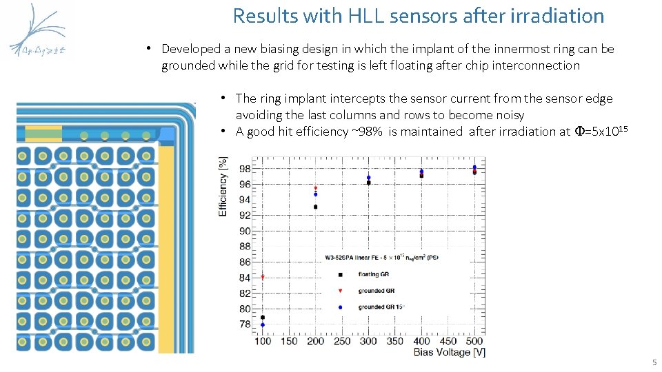
Results with HLL sensors after irradiation • Developed a new biasing design in which the implant of the innermost ring can be grounded while the grid for testing is left floating after chip interconnection • The ring implant intercepts the sensor current from the sensor edge avoiding the last columns and rows to become noisy • A good hit efficiency ~98% is maintained after irradiation at F=5 x 10¹⁵ 5

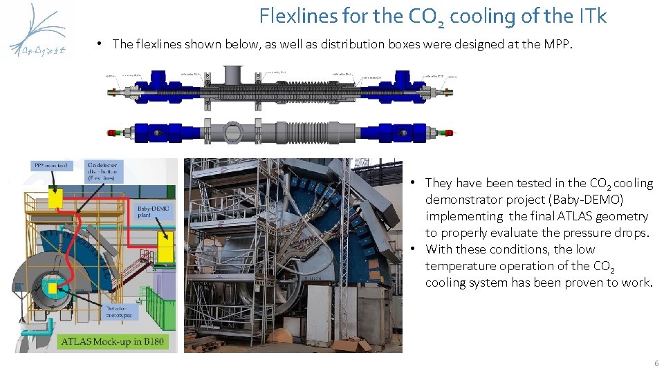
Flexlines for the CO 2 cooling of the ITk • The flexlines shown below, as well as distribution boxes were designed at the MPP. • They have been tested in the CO 2 cooling demonstrator project (Baby-DEMO) implementing the final ATLAS geometry to properly evaluate the pressure drops. • With these conditions, the low temperature operation of the CO 2 cooling system has been proven to work. 6