Laser Diode Principle Laser Diode Principle q Consider
- Slides: 8

Laser Diode Principle

Laser Diode Principle q Consider a p-n junction q In order to design a laser diode, the p-n junction must be heavily doped. q In other word, the p and n materials must be degenerately doped q By degenerated doping, the Fermi level of the n -side will lies in the conduction band whereas the Fermi level in the p-region will lie in the valance band.

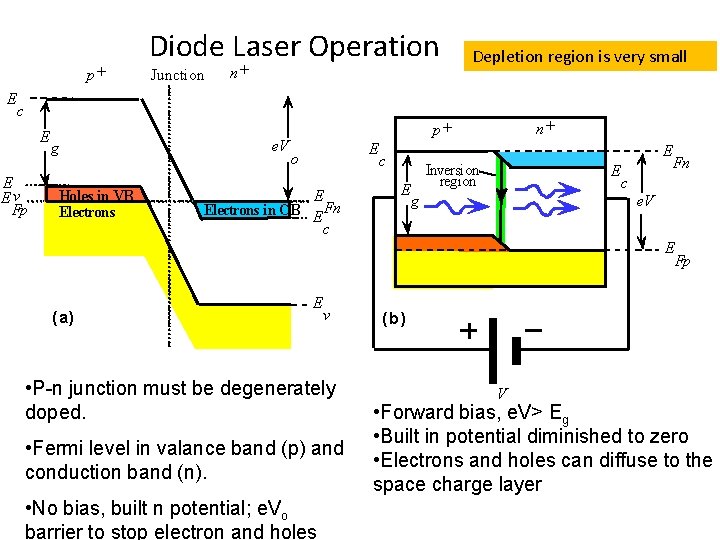
p+ E Diode Laser Operation Junction n+ c E E Ev Fp e. V g Holes in VB Electrons Depletion region is very small n+ p+ E o E Electrons in CB E Fn c E Inversion region E g c Fn e. V E ( a) E v • P-n junction must be degenerately doped. • Fermi level in valance band (p) and conduction band (n). • No bias, built n potential; e. Vo barrier to stop electron and holes Fp (b) V • Forward bias, e. V> Eg • Built in potential diminished to zero • Electrons and holes can diffuse to the space charge layer

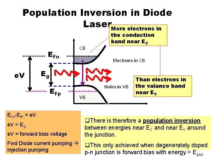
Application of Forward Bias q Suppose that the degenerately doped p-n junction is forward biased by a voltage greater than the band gap; e. V > Eg q The separation between EFn and EFp is now the applied potential energy q The applied voltage diminished the built-in potential barrier, e. Vo to almost zero. q Electrons can now flow to the p-side q Holes can now flow to the n-side

Population Inversion in Diode Laser. More electrons in EFn e. V CB the conduction band near EC Electrons in CB Eg EFp EFn-Ef. P = e. V > Eg e. V = forward bias voltage Fwd Diode current pumping injection pumping Holes in VB VB Than electrons in the valance band near EV q. There is therefore a population inversion between energies near EC and near EV around the junction. q. This only achieved when degenerately doped p-n junction is forward bias with energy > Egap

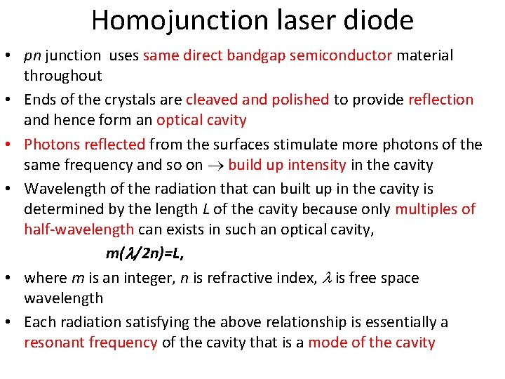
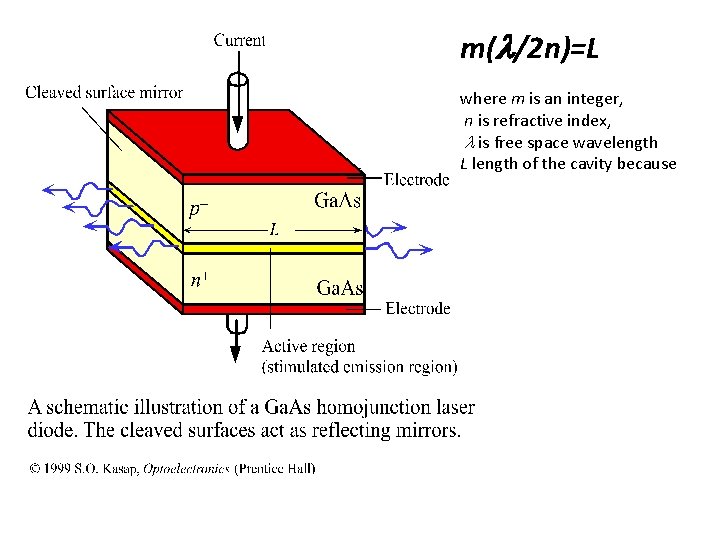
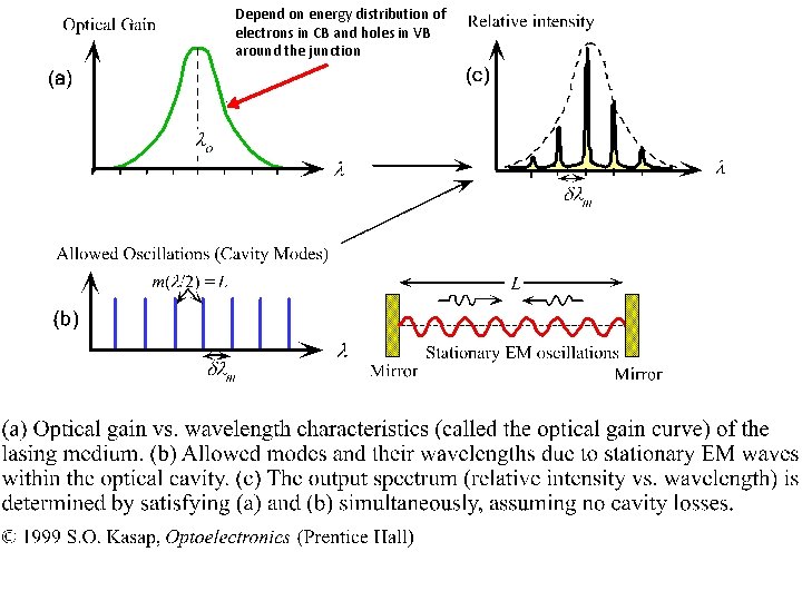
Homojunction laser diode • pn junction uses same direct bandgap semiconductor material throughout • Ends of the crystals are cleaved and polished to provide reflection and hence form an optical cavity • Photons reflected from the surfaces stimulate more photons of the same frequency and so on build up intensity in the cavity • Wavelength of the radiation that can built up in the cavity is determined by the length L of the cavity because only multiples of half-wavelength can exists in such an optical cavity, m( /2 n)=L, • where m is an integer, n is refractive index, is free space wavelength • Each radiation satisfying the above relationship is essentially a resonant frequency of the cavity that is a mode of the cavity

m( /2 n)=L where m is an integer, n is refractive index, is free space wavelength L length of the cavity because

Depend on energy distribution of electrons in CB and holes in VB around the junction