KICK OFF meeting project presentation Mauro DellOrso University
- Slides: 10

KICK OFF meeting - project presentation Mauro Dell’Orso University of Pisa b b m b e t b m b t h e t

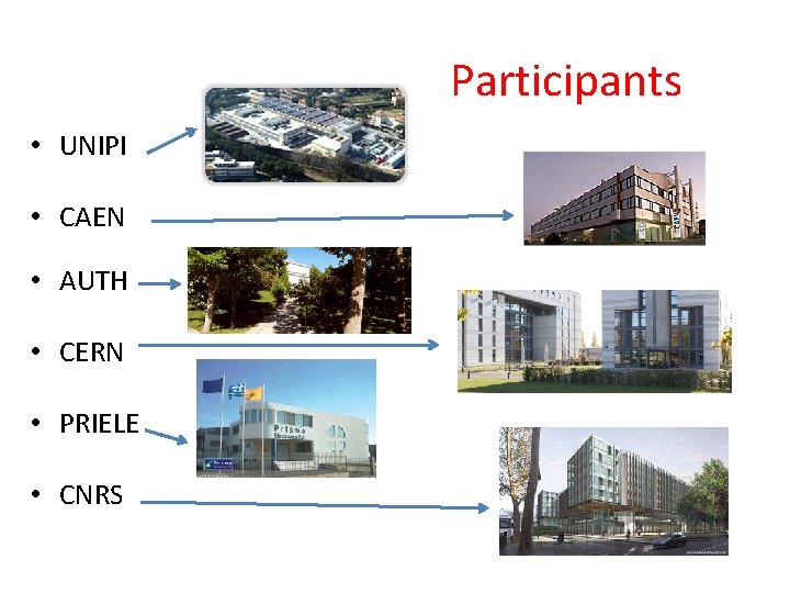
Participants • UNIPI • CAEN • AUTH • CERN • PRIELE • CNRS

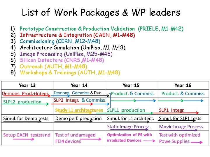
List of Work Packages & WP leaders 1) 2) 3) 4) 5) 6) 7) 8) Prototype Construction & Production Validation (PRIELE, M 1 -M 42) Infrastructure & Integration (CAEN, M 1 -M 48) Commissioning (CERN, M 12 -M 48) Architecture Simulation (Uni. Pisa, M 1 -M 48) Image Processing (Uni. Pisa, M 25 -M 48) Silicon Detectors (CNRS, M 1 -M 48) Outreach (AUTH, M 1 -M 48) Workshops & Trainings (AUTH, M 1 -M 48)

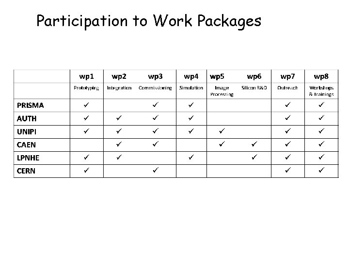
Participation to Work Packages

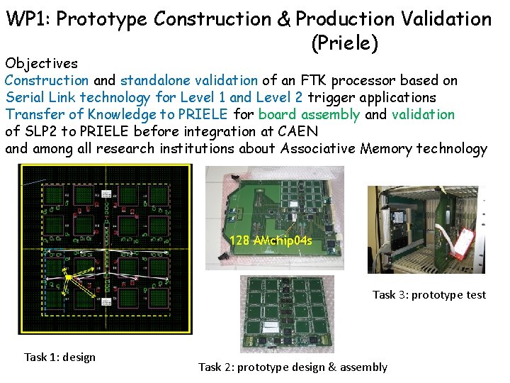
WP 1: Prototype Construction & Production Validation (Priele) Objectives Construction and standalone validation of an FTK processor based on Serial Link technology for Level 1 and Level 2 trigger applications Transfer of Knowledge to PRIELE for board assembly and validation of SLP 2 to PRIELE before integration at CAEN and among all research institutions about Associative Memory technology 128 AMchip 04 s Task 3: prototype test Task 1: design Task 2: prototype design & assembly

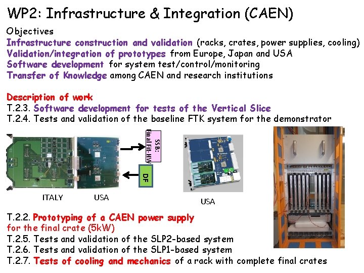
WP 2: Infrastructure & Integration (CAEN) Objectives Infrastructure construction and validation (racks, crates, power supplies, cooling) Validation/integration of prototypes from Europe, Japan and USA Software development for system test/control/monitoring Transfer of Knowledge among CAEN and research institutions Description of work T. 2. 3. Software development for tests of the Vertical Slice T. 2. 4. Tests and validation of the baseline FTK system for the demonstrator SSB: Final Fit-HW DF ITALY USA T. 2. 2. Prototyping of a CAEN power supply for the final crate (5 k. W) T. 2. 5. Tests and validation of the SLP 2 -based system T. 2. 6. Tests and validation of the SLP 1 -based system T. 2. 7. Tests of cooling and mechanics of a rack with complete final crates

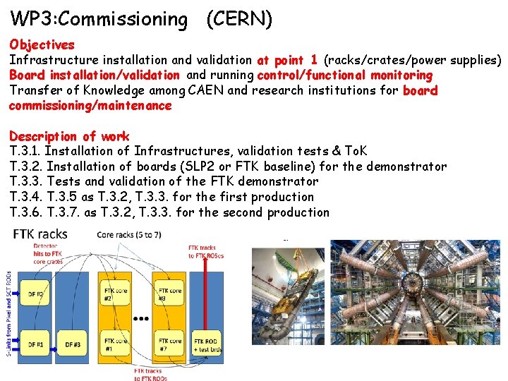
WP 3: Commissioning (CERN) Objectives Infrastructure installation and validation at point 1 (racks/crates/power supplies) Board installation/validation and running control/functional monitoring Transfer of Knowledge among CAEN and research institutions for board commissioning/maintenance Description of work T. 3. 1. Installation of Infrastructures, validation tests & To. K T. 3. 2. Installation of boards (SLP 2 or FTK baseline) for the demonstrator T. 3. 3. Tests and validation of the FTK demonstrator T. 3. 4. T. 3. 5 as T. 3. 2, T. 3. 3. for the first production T. 3. 6. T. 3. 7. as T. 3. 2, T. 3. 3. for the second production

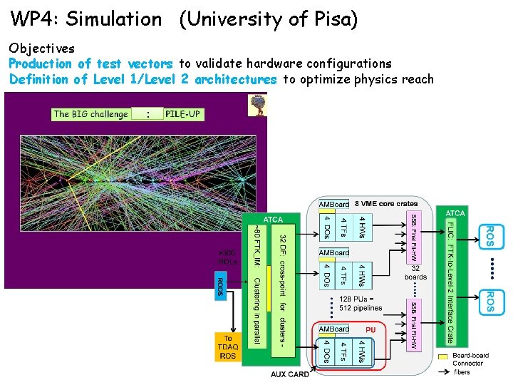
WP 4: Simulation (University of Pisa) Objectives Production of test vectors to validate hardware configurations Definition of Level 1/Level 2 architectures to optimize physics reach :

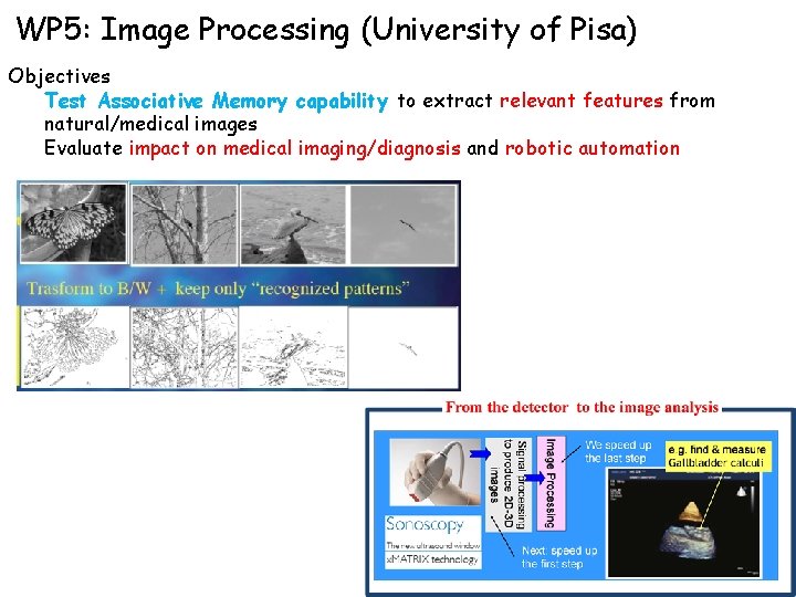
WP 5: Image Processing (University of Pisa) Objectives Test Associative Memory capability to extract relevant features from natural/medical images Evaluate impact on medical imaging/diagnosis and robotic automation

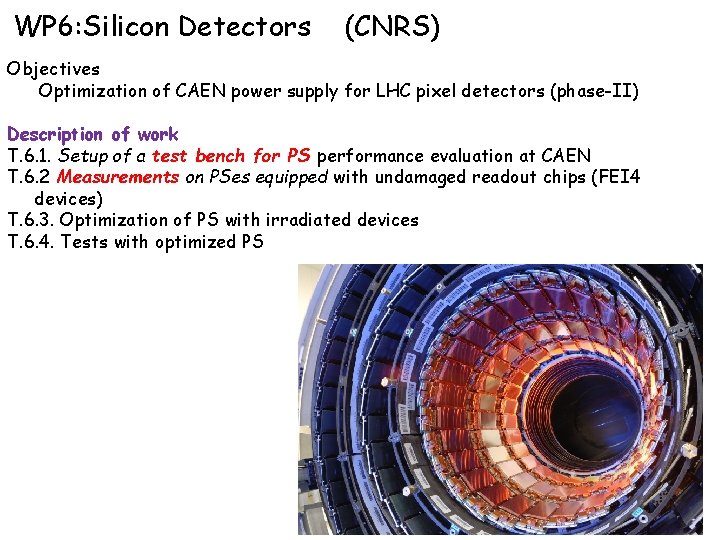
WP 6: Silicon Detectors (CNRS) Objectives Optimization of CAEN power supply for LHC pixel detectors (phase-II) Description of work T. 6. 1. Setup of a test bench for PS performance evaluation at CAEN T. 6. 2 Measurements on PSes equipped with undamaged readout chips (FEI 4 devices) T. 6. 3. Optimization of PS with irradiated devices T. 6. 4. Tests with optimized PS