High efficiency Si solar cells Passivated rear solar
- Slides: 19

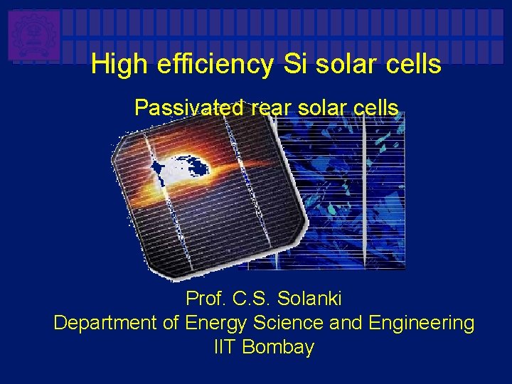
High efficiency Si solar cells Passivated rear solar cells Prof. C. S. Solanki Department of Energy Science and Engineering IIT Bombay

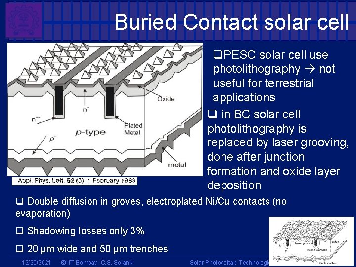
Buried Contact solar cell q. PESC solar cell use photolithography not useful for terrestrial applications q in BC solar cell photolithography is replaced by laser grooving, done after junction formation and oxide layer deposition q Double diffusion in groves, electroplated Ni/Cu contacts (no evaporation) q Shadowing losses only 3% q 20 µm wide and 50 µm trenches 12/25/2021 © IIT Bombay, C. S. Solanki Solar Photovoltaic Technologies 2

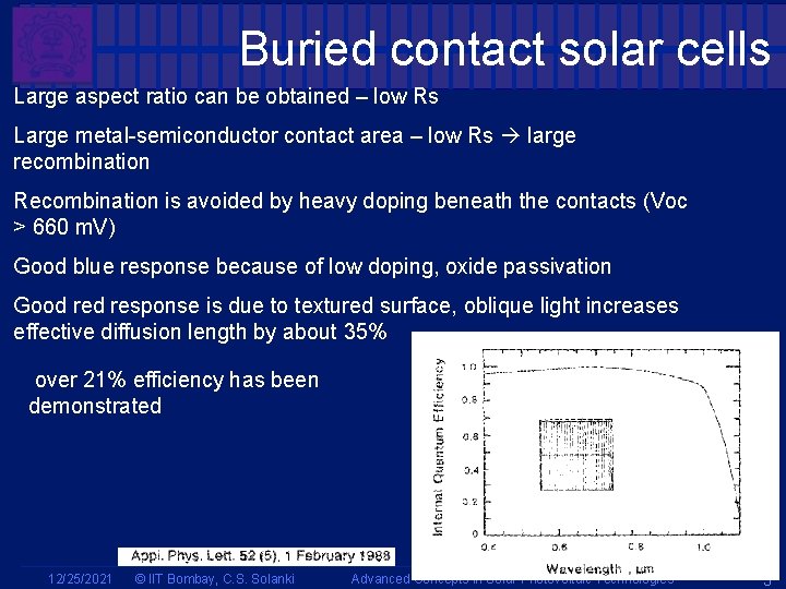
Buried contact solar cells Large aspect ratio can be obtained – low Rs Large metal-semiconductor contact area – low Rs large recombination Recombination is avoided by heavy doping beneath the contacts (Voc > 660 m. V) Good blue response because of low doping, oxide passivation Good response is due to textured surface, oblique light increases effective diffusion length by about 35% over 21% efficiency has been demonstrated 12/25/2021 © IIT Bombay, C. S. Solanki Advanced Concepts in Solar Photovoltaic Technologies 3

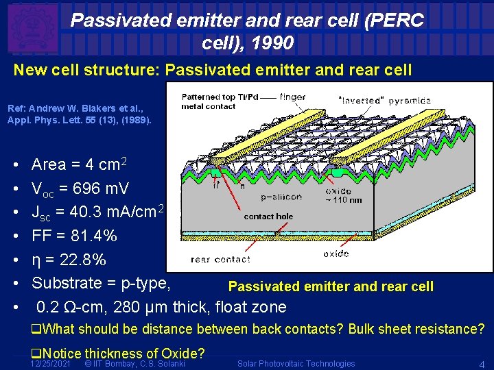
Passivated emitter and rear cell (PERC cell), 1990 New cell structure: Passivated emitter and rear cell Ref: Andrew W. Blakers et al. , Appl. Phys. Lett. 55 (13), (1989). • • Area = 4 cm 2 Voc = 696 m. V Jsc = 40. 3 m. A/cm 2 FF = 81. 4% η = 22. 8% Substrate = p-type, Passivated emitter and rear cell 0. 2 Ω-cm, 280 µm thick, float zone q. What should be distance between back contacts? Bulk sheet resistance? q. Notice thickness of Oxide? 12/25/2021 © IIT Bombay, C. S. Solanki Solar Photovoltaic Technologies 4

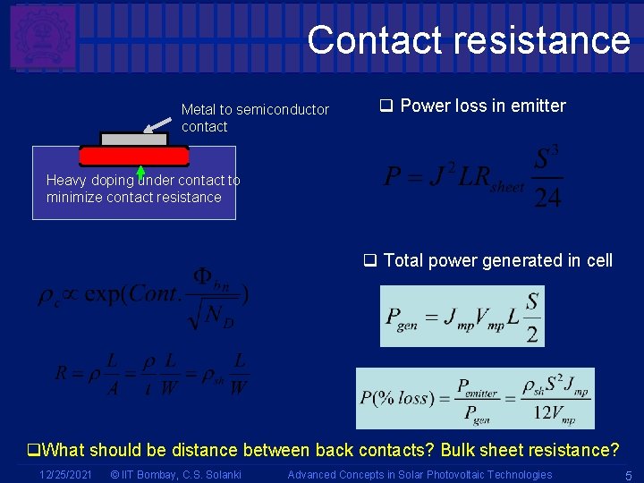
Contact resistance Metal to semiconductor contact q Power loss in emitter Heavy doping under contact to minimize contact resistance q Total power generated in cell q. What should be distance between back contacts? Bulk sheet resistance? 12/25/2021 © IIT Bombay, C. S. Solanki Advanced Concepts in Solar Photovoltaic Technologies 5

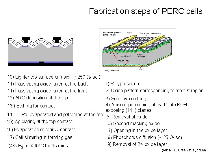
Fabrication steps of PERC cells 10) Lighter top surface diffusion (~250 Ω/ sq ) 11) Passivating oxide layer at the back 11) Passivating oxide layer at the front 12) ARC deposition at the top 1) P- type silicon 2) Oxide pattern corresponding to top flat region 3) Selective etching 4) Anisotropic etching of by Dilute KOH 13 ) Etching for contact exposing (111) planes 14) Ti- Pd, evaporated and patterned at the top 5) Removal of oxide 15) Ag plating at the top contact 6) Second masking oxide 16) Evaporation of rear Al contact 7) Opening in the oxide layer 17) Cell sintering in forming gas 8) Phosphorus diffusion (~ 25 Ω/ sq) (4% H 2) at 400 o. C for 15 mins 9) Removal of 2 nd oxide layer (ref: M. A. Green et al, 1989)

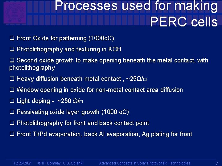
Processes used for making PERC cells q Front Oxide for patterning (1000 o. C) q Photolithography and texturing in KOH q Second oxide growth to make opening beneath the metal contact, with photolithography q Heavy diffusion beneath metal contact , ~25Ω/□ q Window opening in oxide for non-metal contact area diffusion q Light doping - ~250 Ω/□ q Passivating oxide layer growth (1000 o. C) q Photolithography for front and back contact point q Front Ti/Pd evaporation, back Al evaporation, Ag plating for front 12/25/2021 © IIT Bombay, C. S. Solanki Advanced Concepts in Solar Photovoltaic Technologies 7

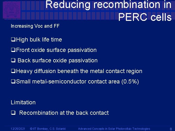
Reducing recombination in PERC cells Increasing Voc and FF q. High bulk life time q. Front oxide surface passivation q Back surface oxide passivation q. Heavy diffusion beneath the metal contact region q. Small metal-semiconductor contact area (0. 5%) Limitation q Recombination at the back contact 12/25/2021 © IIT Bombay, C. S. Solanki Advanced Concepts in Solar Photovoltaic Technologies 8

Increasing current in PERC cells q. High bulk lifetime base, FZ Si q. Inverted pyramid at the top side - Also effective light trapping with good back reflector q. Effective Al reflector at rear - Al/Si reflects 88%, Al/Si. O 2/Si reflects 97% (at 1100 nm) Scope for improvement of PERC cells? - better passivation of back contact -back contact optimization - Reducing resistance from the emitter 12/25/2021 © IIT Bombay, C. S. Solanki Advanced Concepts in Solar Photovoltaic Technologies 9

Passivated emitter and rear cell (PERC cell), 1990 Key difference compared to PESC cell – Top contact: separate doping levels in contacted and non-contacted areas of the top surface – Structural: Large no. of contact holes through passivating oxide layer – Processing: Chlorine based process - improved quality of passivating oxide – Rear Al alloying step (getter bulk region): reduce bulk recombination High Voc • Well passivated surfaces • Lightly phosphorus diffused top surface: reduce surface recombination • High bulk lifetime (minority carrier) Ref: Andrew W. Blakers et al. , Appl. Phys. Lett. 55 (13), (1989). 12/25/2021 © IIT Bombay, C. S. Solanki Solar Photovoltaic Technologies 10

Passivated emitter and rear cell (PERC cell), 1990 High Jsc • Rear Al layer: effective reflector • Inverted pyramid structure: – Reduce reflection – In combination with rear reflector forms light trapping scheme – Superior to upright pyramid • Rear Contact holes: 200 µm dia. on 2 mm x 2 mm matrix Separation distance between the contact area, larger than the thickness of the silicon substrate Ref: Andrew W. Blakers et al. , Appl. Phys. Lett. 55 (13), (1989). 12/25/2021 © IIT Bombay, C. S. Solanki Solar Photovoltaic Technologies 11

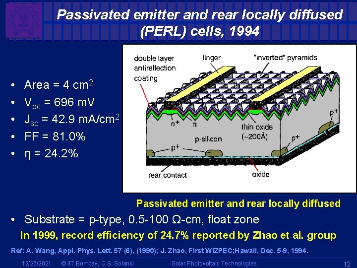
Passivated emitter and rear locally diffused (PERL) cells, 1994 • • • Area = 4 cm 2 Voc = 696 m. V Jsc = 42. 9 m. A/cm 2 FF = 81. 0% η = 24. 2% Passivated emitter and rear locally diffused • Substrate = p-type, 0. 5 -100 Ω-cm, float zone In 1999, record efficiency of 24. 7% reported by Zhao et al. group Ref: A. Wang, Appl. Phys. Lett. 57 (6), (1990); J. Zhao, First WIZPEC; Hawaii, Dec. 5 -9, 1994. 12/25/2021 © IIT Bombay, C. S. Solanki Solar Photovoltaic Technologies 12

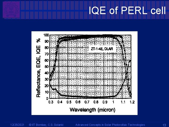
IQE of PERL cell 12/25/2021 © IIT Bombay, C. S. Solanki Advanced Concepts in Solar Photovoltaic Technologies 13

Passivated emitter and rear locally diffused (PERL) cells, 1994 Additional refinement : • Top and bottom contact – Separate doping levels in contacted and non-contacted areas • Reduced recombination – Local diffusion of boron in rear contact – Improved passivation of the Si/Si. O 2 interface at the cell front surface – Atomic H 2 passivation: Improved passivation of thin oxides • Double layer anti-reflection (DLAR) – 3% higher current density than the Si. O 2, single layer antireflection (SLAR) coating • Reduced resistive loss – Two step plating process was used: Increased metal grid conductivity – Zn. S and Mg. F, DLAR coating - Improved EQE (400 -1100 nm) Ref: A. Wang, Appl. Phys. Lett. 57 (6), (1990); J. Zhao, First WIZPEC; Hawaii, Dec. 5 -9, 1994 12/25/2021 © IIT Bombay, C. S. Solanki Solar Photovoltaic Technologies 14

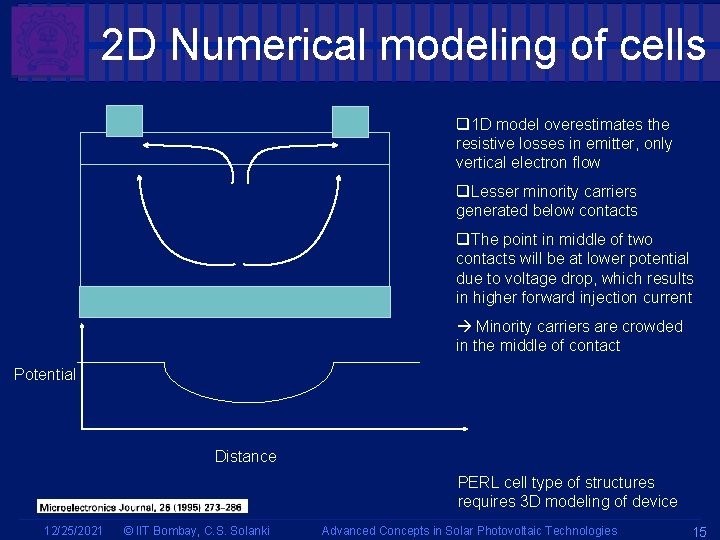
2 D Numerical modeling of cells q 1 D model overestimates the resistive losses in emitter, only vertical electron flow q. Lesser minority carriers generated below contacts q. The point in middle of two contacts will be at lower potential due to voltage drop, which results in higher forward injection current Minority carriers are crowded in the middle of contact Potential Distance PERL cell type of structures requires 3 D modeling of device 12/25/2021 © IIT Bombay, C. S. Solanki Advanced Concepts in Solar Photovoltaic Technologies 15

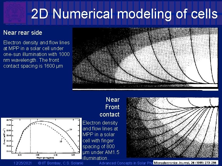
2 D Numerical modeling of cells Near rear side Electron density and flow lines at MPP in a solar cell under one-sun illumination with 1000 nm wavelength. The front contact spacing is 1600 µm Near Front contact Electron density and flow lines at MPP in a solar cell with finger spacing of 800 µm under AM 1. 5 illumination. 12/25/2021 © IIT Bombay, C. S. Solanki Advanced Concepts in Solar Photovoltaic Technologies 16

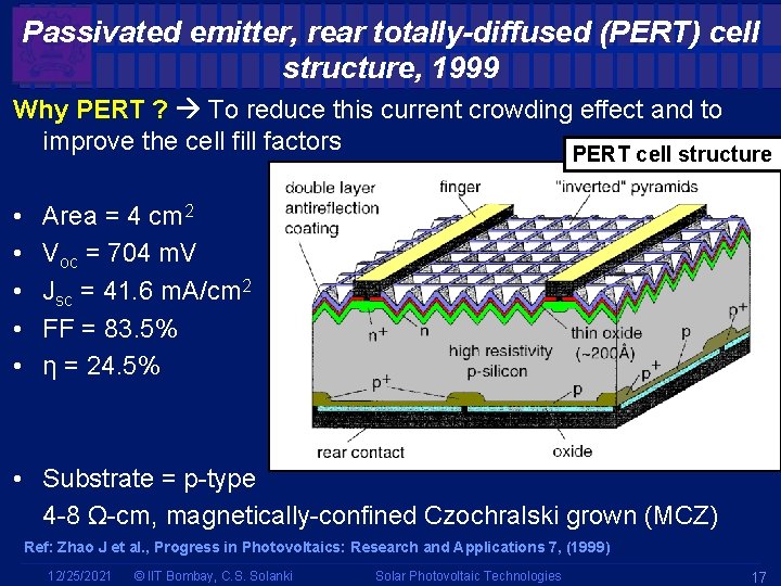
Passivated emitter, rear totally-diffused (PERT) cell structure, 1999 Why PERT ? To reduce this current crowding effect and to improve the cell fill factors PERT cell structure • • • Area = 4 cm 2 Voc = 704 m. V Jsc = 41. 6 m. A/cm 2 FF = 83. 5% η = 24. 5% • Substrate = p-type 4 -8 Ω-cm, magnetically-confined Czochralski grown (MCZ) Ref: Zhao J et al. , Progress in Photovoltaics: Research and Applications 7, (1999) 12/25/2021 © IIT Bombay, C. S. Solanki Solar Photovoltaic Technologies 17

Passivated emitter, rear totally-diffused (PERT) cell structure, 1999 Difference between PERL and PERT • Lightly boron diffused layer along the entire rear surface of the PERT cell Ref: Zhao J et al. , Progress in Photovoltaics: Research and Applications 7, (1999) 12/25/2021 © IIT Bombay, C. S. Solanki Solar Photovoltaic Technologies 18

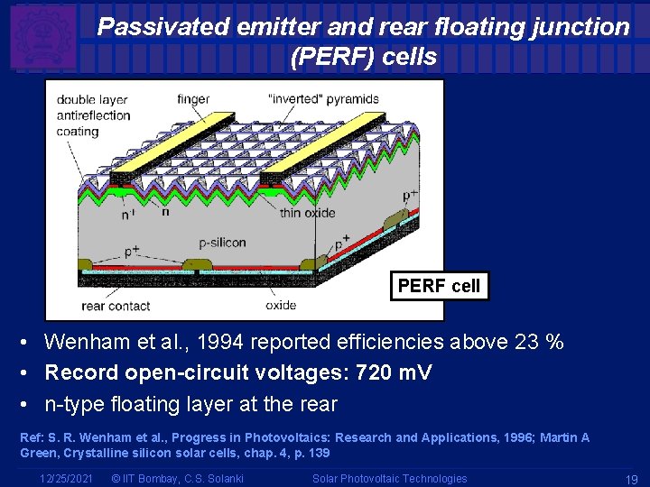
Passivated emitter and rear floating junction (PERF) cells PERF cell • Wenham et al. , 1994 reported efficiencies above 23 % • Record open-circuit voltages: 720 m. V • n-type floating layer at the rear Ref: S. R. Wenham et al. , Progress in Photovoltaics: Research and Applications, 1996; Martin A Green, Crystalline silicon solar cells, chap. 4, p. 139 12/25/2021 © IIT Bombay, C. S. Solanki Solar Photovoltaic Technologies 19