ENEE 303 1 st Discussion SelfIntroduction Name Yusen


 – is influenced by two factors: –")


 active mode with VCE = 5")
- Slides: 18
ENEE 303 1 st Discussion
Self-Introduction • Name: Yusen Fan • Email: ysfan@umd. edu • Office Hour: Tuesdays 10 -12 @ AVW 1143
Contents • Pspice demonstration • Diode, BJT overview
Pspice • Tutorial: https: //engineering. purdue. edu/~ee 255/lec turesupp_files/PSpice-Tutorial. pdf
Pspice diode and transistor models • Can be found on the course website • e. g. – PSpice diode model for 1 N 4007 – PSpice models for BJT 2 N 390 x transistors
Diode Bipolar Junction Transistors ENEE 303 Fall 2016
Current-Voltage Relationship of a pn-Junction
Example 4. 2: Multiple Diodes
Small-Signal Model • Q: How is small-signal resistance rd defined? • (Slope at the Q point) – A: From steady-state current (ID) and thermal voltage (VT) as below. • Note this approximation is only valid for smallsignal voltages vd < 5 m. V.
Small-Signal Model • Consider the circuit shown above for the case in which R = 10 k. Ohm. • The power supply V+ has a dc value of 10 V over which is superimposed a 60 Hz sinusoid of 1 V peak amplitude (known as the supply ripple) – Q: Calculate both amplitude of the sine-wave signal observed across the diode. • A: vd. (peak) = 2. 68 m. V • Assume diode to have 0. 7 V drop at 1 m. A current.
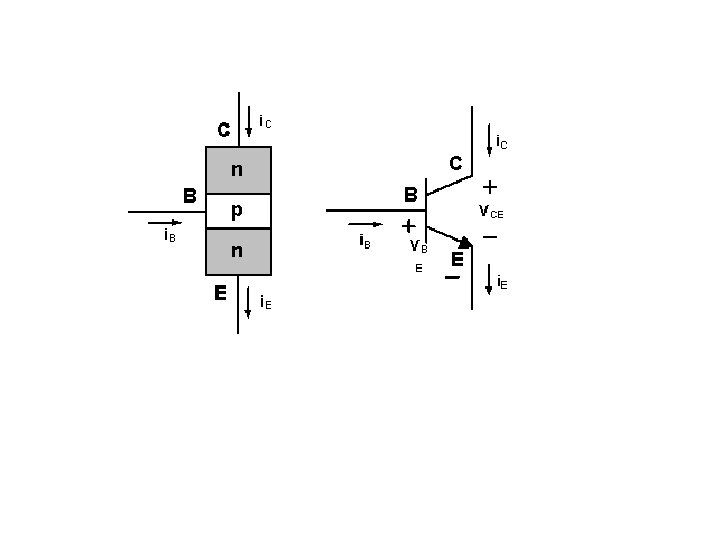
BJT Bipolar Junction Transistors ENEE 303 Fall 2016
• common-emitter current gain (b. ) – is influenced by two factors: – width of base region (W) – relative doping of base emitter regions (NA/ND) • High Value of b – thin base (small W in nano-meters) – lightly doped base / heavily doped emitter (small NA/ND)
• All current which enters transistor must leave. • When combined with equations from the previous slides
i. C – v. BE Characteristic for an npn Transistor
Operation regions of BJT 1. Active mode: BE forward biased, CB reverse biased 2. Saturation mode: BE, CB are both forward biased 3. Cut off mode: BE, CB reverse biased
Models for the Operation of the npn BJT in Various Modes npn transistor active mode cutoff mode saturation mode
Example 6. 3 Find VBB to achieve, a) active mode with VCE = 5 V Assume VBE = 0. 7 V and b = 50. a)