EECS 361 Computer Architecture Lecture 16 Memory Systems
- Slides: 22

EECS 361 Computer Architecture Lecture 16: Memory Systems memory. 1

Outline of Today’s Lecture ° Recap and Introduction ° Memory System: the BIG Picture? ° Questions and Administrative Matters ° Memory Technology: SRAM ° Memory Technology: DRAM ° A Real Life Example: SPARCstation 20’s Memory System ° Summary memory. 4

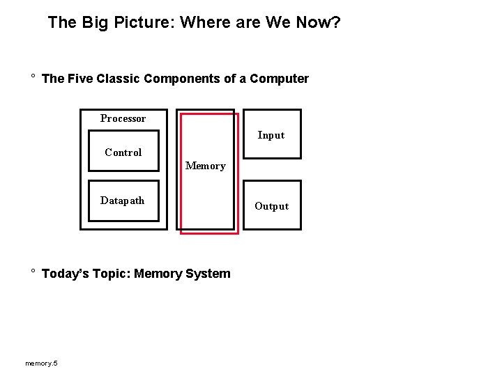
The Big Picture: Where are We Now? ° The Five Classic Components of a Computer Processor Input Control Memory Datapath ° Today’s Topic: Memory System memory. 5 Output

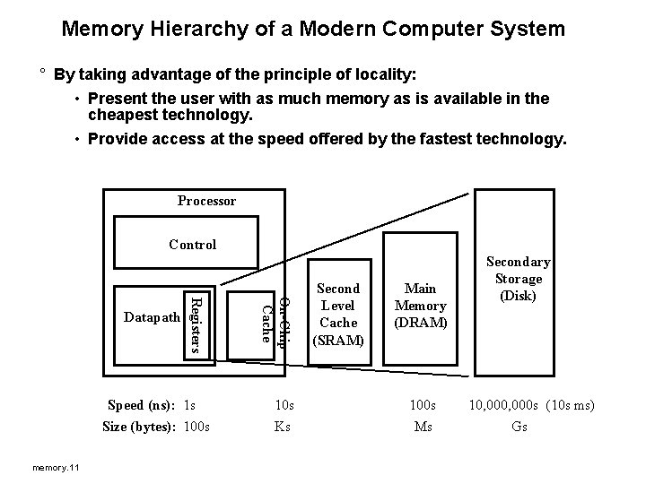
Memory Hierarchy of a Modern Computer System ° By taking advantage of the principle of locality: • Present the user with as much memory as is available in the cheapest technology. • Provide access at the speed offered by the fastest technology. Processor Control Speed (ns): 1 s Size (bytes): 100 s memory. 11 On-Chip Cache Registers Datapath 10 s Ks Second Level Cache (SRAM) Main Memory (DRAM) 100 s Ms Secondary Storage (Disk) 10, 000 s (10 s ms) Gs

Memory Hierarchy Technology ° Random Access: • “Random” is good: access time is the same for all locations • DRAM: Dynamic Random Access Memory - High density, low power, cheap, slow - Dynamic: need to be “refreshed” regularly • SRAM: Static Random Access Memory - Low density, high power, expensive, fast - Static: content will last “forever” ° “Non-so-random” Access Technology: • Access time varies from location to location and from time to time • Examples: Disk, tape drive, CDROM memory. 12

Random Access Memory (RAM) Technology ° Why do computer designers need to know about RAM technology? • Processor performance is usually limited by memory bandwidth • As IC densities increase, lots of memory will fit on processor chip - Tailor on-chip memory to specific needs - Instruction cache - Data cache - Write buffer ° What makes RAM different from a bunch of flip-flops? • Density: RAM is much more denser memory. 13

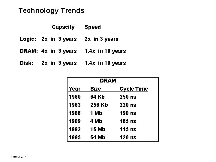
Technology Trends Capacity Logic: 2 x in 3 years Speed 2 x in 3 years DRAM: 4 x in 3 years 1. 4 x in 10 years Disk: 1. 4 x in 10 years 2 x in 3 years DRAM memory. 14 Year 1980 1983 1986 Size 64 Kb 256 Kb 1 Mb Cycle Time 250 ns 220 ns 1989 1992 1995 4 Mb 16 Mb 64 Mb 165 ns 145 ns 120 ns

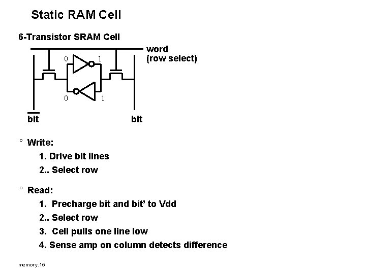
Static RAM Cell 6 -Transistor SRAM Cell 0 0 word (row select) 1 1 bit ° Write: 1. Drive bit lines 2. . Select row ° Read: 1. Precharge bit and bit’ to Vdd 2. . Select row 3. Cell pulls one line low 4. Sense amp on column detects difference memory. 15

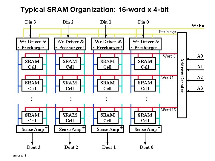
Typical SRAM Organization: 16 -word x 4 -bit Din 3 Din 2 Din 1 Din 0 Wr. En Precharge Wr Driver & - Precharger + SRAM Cell Word 1 SRAM Cell : : Word 15 SRAM Cell - Sense Amp + Dout 3 Dout 2 Dout 1 Dout 0 memory. 16 Address Decoder Word 0 A 1 A 2 A 3

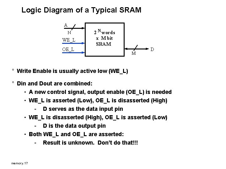
Logic Diagram of a Typical SRAM A N WE_L OE_L 2 N words x M bit SRAM M D ° Write Enable is usually active low (WE_L) ° Din and Dout are combined: • A new control signal, output enable (OE_L) is needed • WE_L is asserted (Low), OE_L is disasserted (High) - D serves as the data input pin • WE_L is disasserted (High), OE_L is asserted (Low) - D is the data output pin • Both WE_L and OE_L are asserted: - Result is unknown. Don’t do that!!! memory. 17

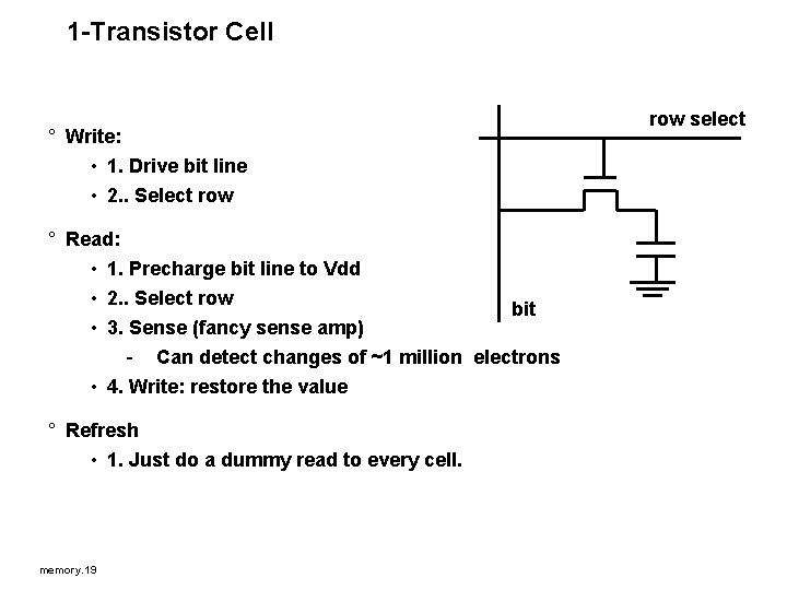
1 -Transistor Cell ° Write: • 1. Drive bit line • 2. . Select row ° Read: • 1. Precharge bit line to Vdd • 2. . Select row bit • 3. Sense (fancy sense amp) - Can detect changes of ~1 million electrons • 4. Write: restore the value ° Refresh • 1. Just do a dummy read to every cell. memory. 19 row select

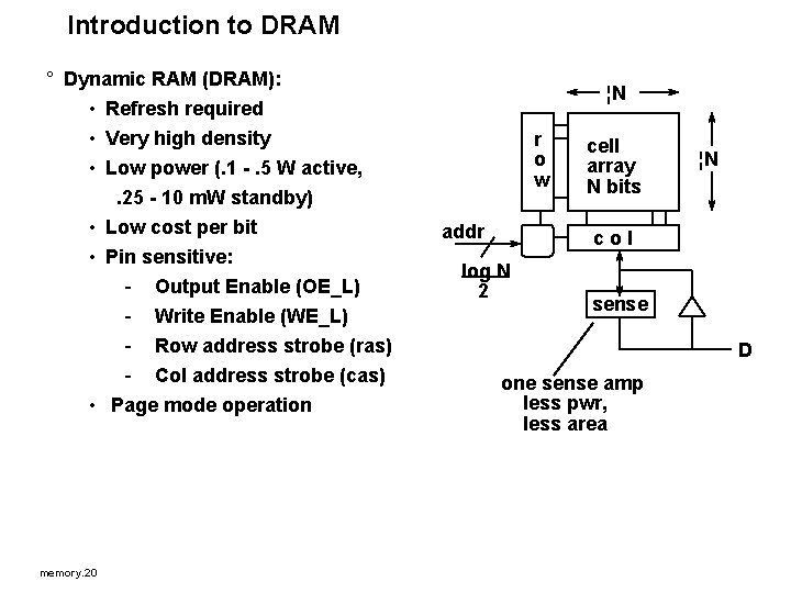
Introduction to DRAM ° Dynamic RAM (DRAM): • Refresh required • Very high density • Low power (. 1 -. 5 W active, . 25 - 10 m. W standby) • Low cost per bit • Pin sensitive: - Output Enable (OE_L) - Write Enable (WE_L) - Row address strobe (ras) - Col address strobe (cas) • Page mode operation memory. 20 ¦N r o w addr cell array N bits ¦N col log N 2 sense D one sense amp less pwr, less area

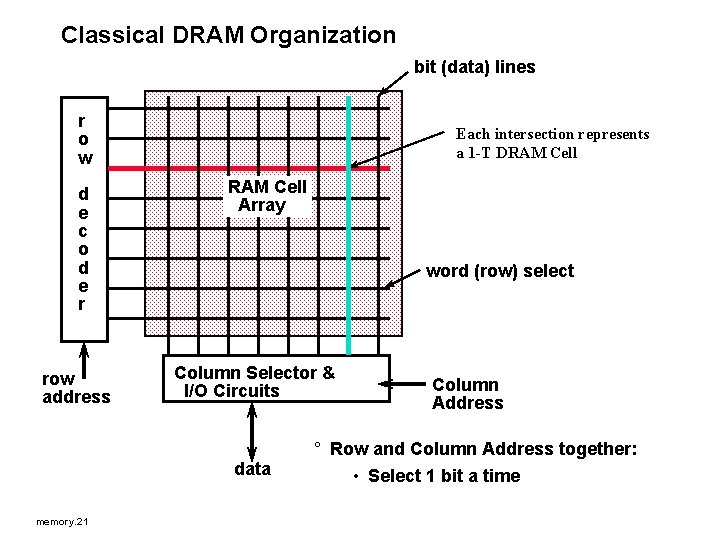
Classical DRAM Organization bit (data) lines r o w d e c o d e r row address Each intersection represents a 1 -T DRAM Cell Array word (row) select Column Selector & I/O Circuits data memory. 21 Column Address ° Row and Column Address together: • Select 1 bit a time

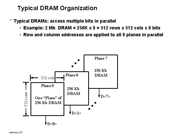
Typical DRAM Organization ° Typical DRAMs: access multiple bits in parallel • Example: 2 Mb DRAM = 256 K x 8 = 512 rows x 512 cols x 8 bits • Row and column addresses are applied to all 8 planes in parallel Plane 7 512 cols 512 rows Plane 0 One “Plane” of 256 Kb DRAM Plane 0 256 Kb DRAM D<1> D<0> memory. 22 256 Kb DRAM D<7>

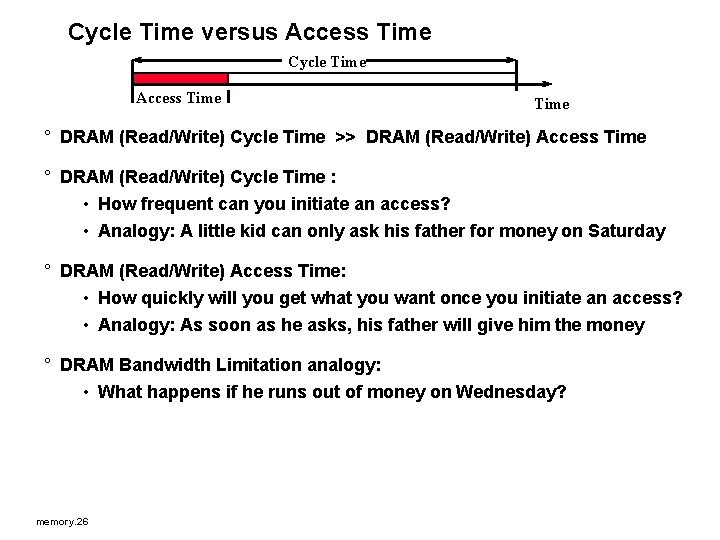
Cycle Time versus Access Time Cycle Time Access Time ° DRAM (Read/Write) Cycle Time >> DRAM (Read/Write) Access Time ° DRAM (Read/Write) Cycle Time : • How frequent can you initiate an access? • Analogy: A little kid can only ask his father for money on Saturday ° DRAM (Read/Write) Access Time: • How quickly will you get what you want once you initiate an access? • Analogy: As soon as he asks, his father will give him the money ° DRAM Bandwidth Limitation analogy: • What happens if he runs out of money on Wednesday? memory. 26

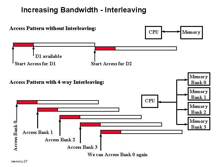
Increasing Bandwidth - Interleaving Access Pattern without Interleaving: D 1 available Start Access for D 1 CPU Memory Start Access for D 2 Memory Bank 0 Access Pattern with 4 -way Interleaving: CPU Memory Bank 1 Access Bank 0 Memory Bank 2 Access Bank 1 Access Bank 2 Access Bank 3 We can Access Bank 0 again memory. 27 Memory Bank 3

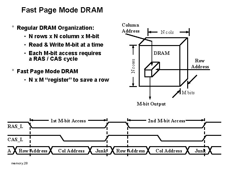
Fast Page Mode DRAM ° Fast Page Mode DRAM • N x M “register” to save a row Column Address N cols DRAM Row Address N rows ° Regular DRAM Organization: • N rows x N column x M-bit • Read & Write M-bit at a time • Each M-bit access requires a RAS / CAS cycle M bits M-bit Output 1 st M-bit Access 2 nd M-bit Access RAS_L CAS_L A Row Address memory. 28 Col Address Junk Row Address Col Address Junk

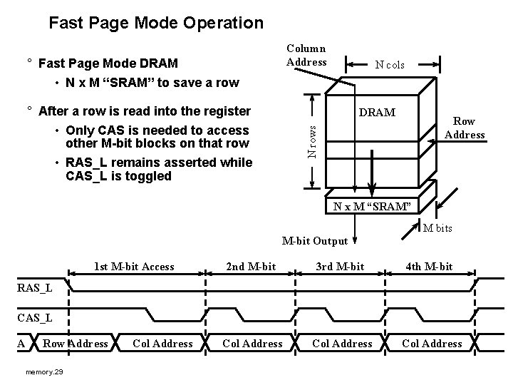
Fast Page Mode Operation ° After a row is read into the register • Only CAS is needed to access other M-bit blocks on that row • RAS_L remains asserted while CAS_L is toggled N cols DRAM Row Address N rows ° Fast Page Mode DRAM • N x M “SRAM” to save a row Column Address N x M “SRAM” M bits M-bit Output 1 st M-bit Access 2 nd M-bit 3 rd M-bit 4 th M-bit Col Address RAS_L CAS_L A Row Address memory. 29 Col Address

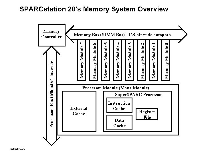
SPARCstation 20’s Memory System Overview memory. 30 Processor Module (Mbus Module) Super. SPARC Processor External Cache Instruction Cache Data Cache Register File Memory Module 0 Memory Module 1 Memory Module 2 Memory Module 3 Memory Module 4 Memory Module 5 Memory Module 6 Memory Bus (SIMM Bus) 128 -bit wide datapath Memory Module 7 Processor Bus (Mbus) 64 -bit wide Memory Controller

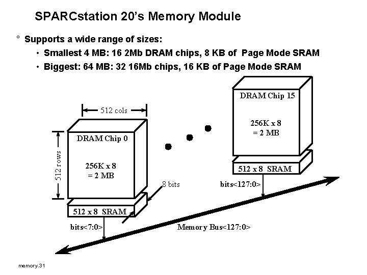
SPARCstation 20’s Memory Module ° Supports a wide range of sizes: • Smallest 4 MB: 16 2 Mb DRAM chips, 8 KB of Page Mode SRAM • Biggest: 64 MB: 32 16 Mb chips, 16 KB of Page Mode SRAM DRAM Chip 15 512 cols 256 K x 8 = 2 MB 512 rows DRAM Chip 0 256 K x 8 = 2 MB 512 x 8 SRAM 8 bits<127: 0> 512 x 8 SRAM bits<7: 0> memory. 31 Memory Bus<127: 0>

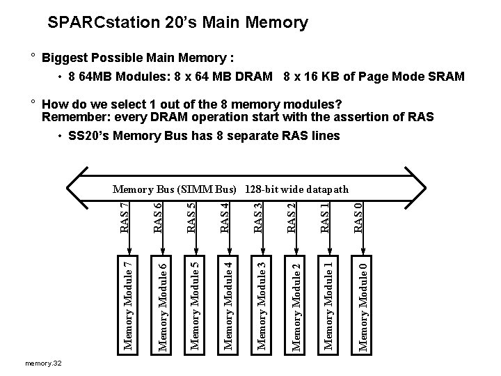
SPARCstation 20’s Main Memory ° Biggest Possible Main Memory : • 8 64 MB Modules: 8 x 64 MB DRAM 8 x 16 KB of Page Mode SRAM ° How do we select 1 out of the 8 memory modules? Remember: every DRAM operation start with the assertion of RAS • SS 20’s Memory Bus has 8 separate RAS lines memory. 32 RAS 0 Memory Module 0 RAS 1 Memory Module 1 RAS 2 Memory Module 2 RAS 3 Memory Module 3 RAS 4 Memory Module 4 RAS 5 Memory Module 5 RAS 6 Memory Module 7 RAS 7 Memory Bus (SIMM Bus) 128 -bit wide datapath

Summary: ° Two Different Types of Locality: • Temporal Locality (Locality in Time): If an item is referenced, it will tend to be referenced again soon. • Spatial Locality (Locality in Space): If an item is referenced, items whose addresses are close by tend to be referenced soon. ° By taking advantage of the principle of locality: • Present the user with as much memory as is available in the cheapest technology. • Provide access at the speed offered by the fastest technology. ° DRAM is slow but cheap and dense: • Good choice for presenting the user with a BIG memory system ° SRAM is fast but expensive and not very dense: • Good choice for providing the user FAST access time. memory. 33