361 Computer Architecture Lecture 15 Cache Memory cache
- Slides: 19

361 Computer Architecture Lecture 15: Cache Memory cache. 1

Outline of Today’s Lecture ° Cache Replacement Policy ° Cache Write Policy ° Example ° Summary cache. 2

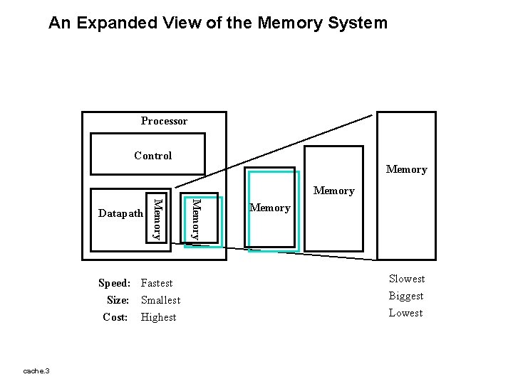
An Expanded View of the Memory System Processor Control Memory Speed: Fastest Size: Smallest Cost: Highest cache. 3 Memory Datapath Memory Slowest Biggest Lowest

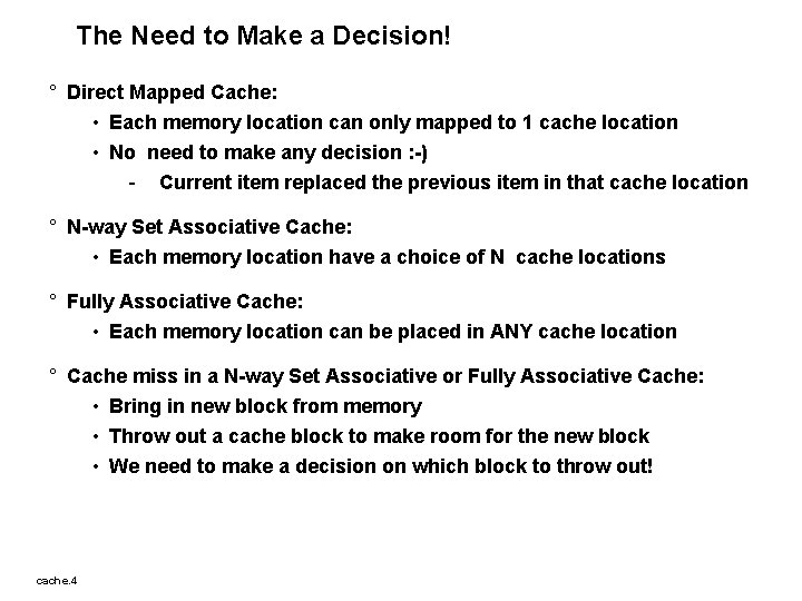
The Need to Make a Decision! ° Direct Mapped Cache: • Each memory location can only mapped to 1 cache location • No need to make any decision : -) - Current item replaced the previous item in that cache location ° N-way Set Associative Cache: • Each memory location have a choice of N cache locations ° Fully Associative Cache: • Each memory location can be placed in ANY cache location ° Cache miss in a N-way Set Associative or Fully Associative Cache: • Bring in new block from memory • Throw out a cache block to make room for the new block • We need to make a decision on which block to throw out! cache. 4

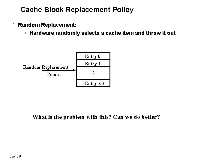
Cache Block Replacement Policy ° Random Replacement: • Hardware randomly selects a cache item and throw it out Random Replacement Pointer Entry 0 Entry 1 : Entry 63 What is the problem with this? Can we do better? cache. 5

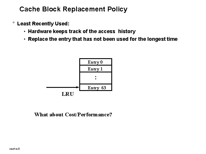
Cache Block Replacement Policy ° Least Recently Used: • Hardware keeps track of the access history • Replace the entry that has not been used for the longest time Entry 0 Entry 1 : Entry 63 LRU What about Cost/Performance? cache. 6

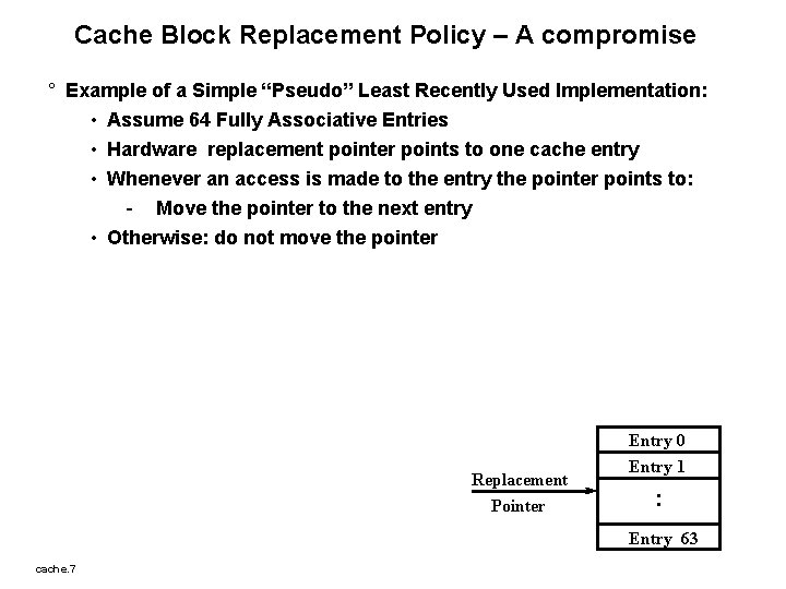
Cache Block Replacement Policy – A compromise ° Example of a Simple “Pseudo” Least Recently Used Implementation: • Assume 64 Fully Associative Entries • Hardware replacement pointer points to one cache entry • Whenever an access is made to the entry the pointer points to: - Move the pointer to the next entry • Otherwise: do not move the pointer Replacement Pointer Entry 0 Entry 1 : Entry 63 cache. 7

Cache Write Policy: Write Through versus Write Back ° Cache read is much easier to handle than cache write: • Instruction cache is much easier to design than data cache ° Cache write: • How do we keep data in the cache and memory consistent? ° Two options (decision time again : -) • Write Back: write to cache only. Write the cache block to memory when that cache block is being replaced on a cache miss. - Need a “dirty” bit for each cache block - Greatly reduce the memory bandwidth requirement - Control can be complex • Write Through: write to cache and memory at the same time. - What!!! How can this be? Isn’t memory too slow for this? cache. 8

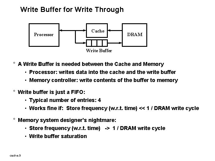
Write Buffer for Write Through Processor Cache DRAM Write Buffer ° A Write Buffer is needed between the Cache and Memory • Processor: writes data into the cache and the write buffer • Memory controller: write contents of the buffer to memory ° Write buffer is just a FIFO: • Typical number of entries: 4 • Works fine if: Store frequency (w. r. t. time) << 1 / DRAM write cycle ° Memory system designer’s nightmare: • Store frequency (w. r. t. time) -> 1 / DRAM write cycle • Write buffer saturation cache. 9

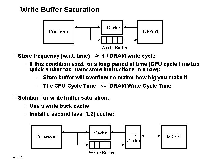
Write Buffer Saturation Processor Cache DRAM Write Buffer ° Store frequency (w. r. t. time) -> 1 / DRAM write cycle • If this condition exist for a long period of time (CPU cycle time too quick and/or too many store instructions in a row): - Store buffer will overflow no matter how big you make it - The CPU Cycle Time <= DRAM Write Cycle Time ° Solution for write buffer saturation: • Use a write back cache • Install a second level (L 2) cache: Processor Cache Write Buffer cache. 10 L 2 Cache DRAM

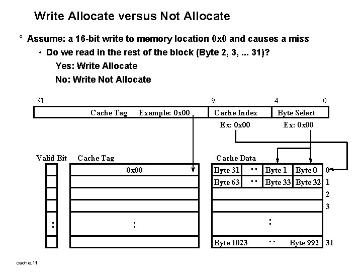
Write Allocate versus Not Allocate ° Assume: a 16 -bit write to memory location 0 x 0 and causes a miss • Do we read in the rest of the block (Byte 2, 3, . . . 31)? Yes: Write Allocate No: Write Not Allocate Valid Bit Example: 0 x 00 Cache Tag 0 x 00 : Cache Data Byte 31 Byte 63 Byte 1 Byte 0 0 Byte 33 Byte 32 1 2 3 : : Byte 1023 cache. 11 4 0 Byte Select Ex: 0 x 00 : Cache Tag 9 Cache Index Ex: 0 x 00 : : 31 Byte 992 31

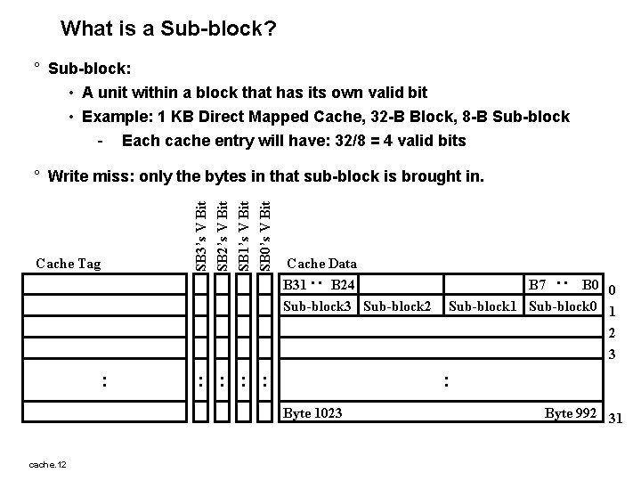
What is a Sub-block? ° Sub-block: • A unit within a block that has its own valid bit • Example: 1 KB Direct Mapped Cache, 32 -B Block, 8 -B Sub-block - Each cache entry will have: 32/8 = 4 valid bits : : Byte 1023 cache. 12 B 7 B 0 0 Sub-block 1 Sub-block 0 1 2 3 : Cache Data B 31 B 24 Sub-block 3 Sub-block 2 : Cache Tag SB 1’s V Bit SB 0’s V Bit SB 3’s V Bit SB 2’s V Bit ° Write miss: only the bytes in that sub-block is brought in. Byte 992 31

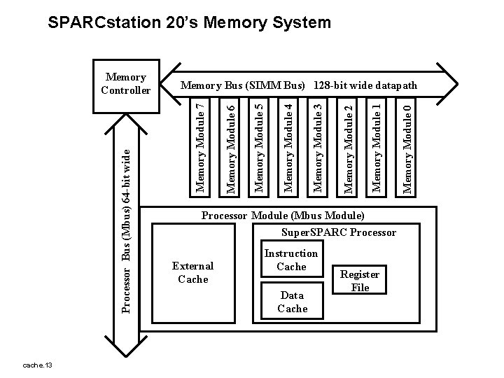
SPARCstation 20’s Memory System cache. 13 Processor Module (Mbus Module) Super. SPARC Processor External Cache Instruction Cache Data Cache Register File Memory Module 0 Memory Module 1 Memory Module 2 Memory Module 3 Memory Module 4 Memory Module 5 Memory Module 6 Memory Bus (SIMM Bus) 128 -bit wide datapath Memory Module 7 Processor Bus (Mbus) 64 -bit wide Memory Controller

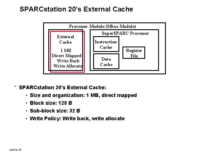
SPARCstation 20’s External Cache Processor Module (Mbus Module) Super. SPARC Processor External Instruction Cache 1 MB Register Direct Mapped File Data Write Back Cache Write Allocate ° SPARCstation 20’s External Cache: • Size and organization: 1 MB, direct mapped • Block size: 128 B • Sub-block size: 32 B • Write Policy: Write back, write allocate cache. 14

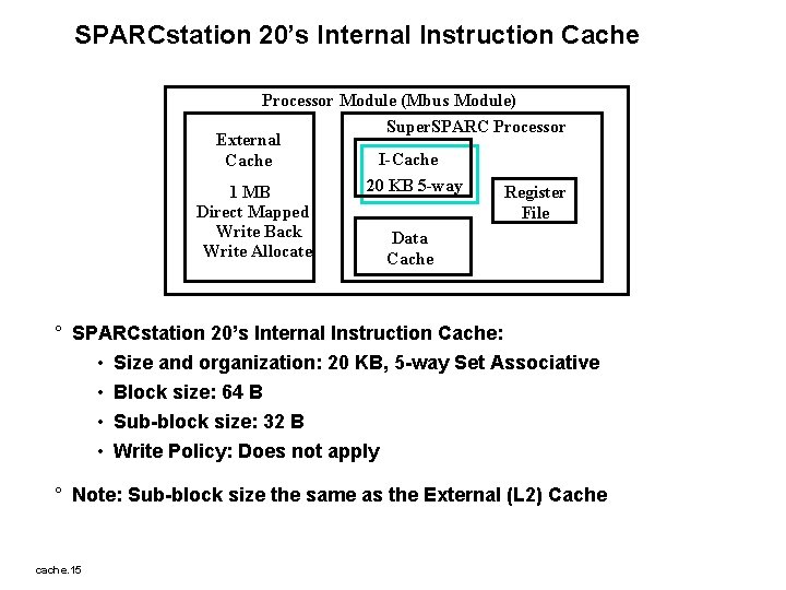
SPARCstation 20’s Internal Instruction Cache Processor Module (Mbus Module) Super. SPARC Processor External I-Cache 20 KB 5 -way 1 MB Register Direct Mapped File Write Back Data Write Allocate Cache ° SPARCstation 20’s Internal Instruction Cache: • Size and organization: 20 KB, 5 -way Set Associative • Block size: 64 B • Sub-block size: 32 B • Write Policy: Does not apply ° Note: Sub-block size the same as the External (L 2) Cache cache. 15

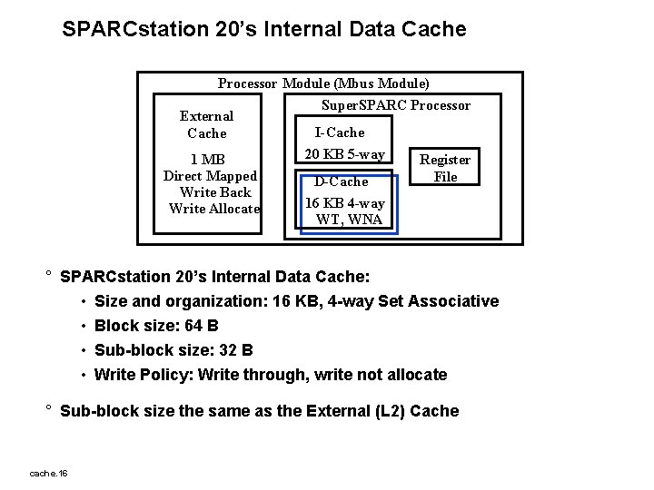
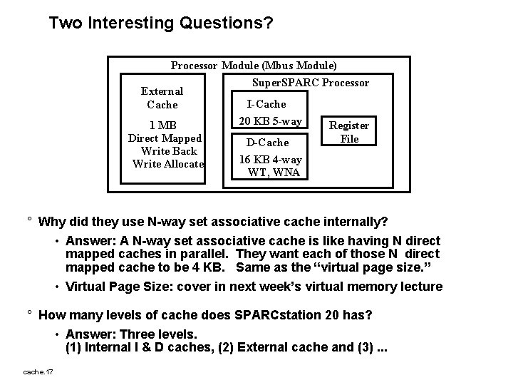
SPARCstation 20’s Internal Data Cache Processor Module (Mbus Module) Super. SPARC Processor External I-Cache 20 KB 5 -way 1 MB Register Direct Mapped File D-Cache Write Back 16 KB 4 -way Write Allocate WT, WNA ° SPARCstation 20’s Internal Data Cache: • Size and organization: 16 KB, 4 -way Set Associative • Block size: 64 B • Sub-block size: 32 B • Write Policy: Write through, write not allocate ° Sub-block size the same as the External (L 2) Cache cache. 16

Two Interesting Questions? Processor Module (Mbus Module) Super. SPARC Processor External I-Cache 20 KB 5 -way 1 MB Register Direct Mapped File D-Cache Write Back 16 KB 4 -way Write Allocate WT, WNA ° Why did they use N-way set associative cache internally? • Answer: A N-way set associative cache is like having N direct mapped caches in parallel. They want each of those N direct mapped cache to be 4 KB. Same as the “virtual page size. ” • Virtual Page Size: cover in next week’s virtual memory lecture ° How many levels of cache does SPARCstation 20 has? • Answer: Three levels. (1) Internal I & D caches, (2) External cache and (3). . . cache. 17

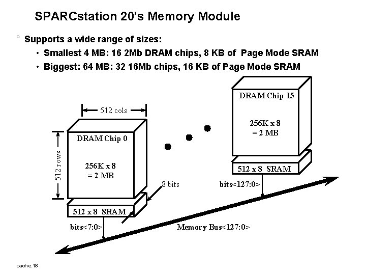
SPARCstation 20’s Memory Module ° Supports a wide range of sizes: • Smallest 4 MB: 16 2 Mb DRAM chips, 8 KB of Page Mode SRAM • Biggest: 64 MB: 32 16 Mb chips, 16 KB of Page Mode SRAM DRAM Chip 15 512 cols 256 K x 8 = 2 MB 512 rows DRAM Chip 0 256 K x 8 = 2 MB 512 x 8 SRAM 8 bits<127: 0> 512 x 8 SRAM bits<7: 0> cache. 18 Memory Bus<127: 0>

Summary: ° Replacement Policy • Exploit principle of locality ° Write Policy: • Write Through: need a write buffer. Nightmare: WB saturation • Write Back: control can be complex ° Getting data into the processor from Cache and into the cache from slower memory are one of the most important R&D topics in industry. cache. 19