Digital Signal Processing at 1 GHz in a

- Slides: 30
Digital Signal Processing at 1 GHz in a Field-Programmable Object Array Dirk Helgemo Chief Architect Math. Star, Inc. 24 September 2003 1
Contents • Driving Philosophy • Architecture – Communication – Object Types • • DSP Algorithms in Objects Tools Applications Roadmap 2
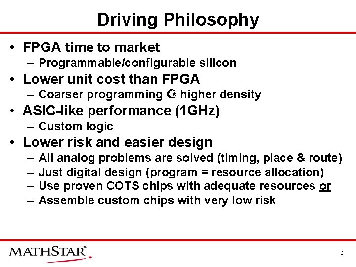
Driving Philosophy • FPGA time to market – Programmable/configurable silicon • Lower unit cost than FPGA – Coarser programming higher density • ASIC-like performance (1 GHz) – Custom logic • Lower risk and easier design – – All analog problems are solved (timing, place & route) Just digital design (program = resource allocation) Use proven COTS chips with adequate resources or Assemble custom chips with very low risk 3
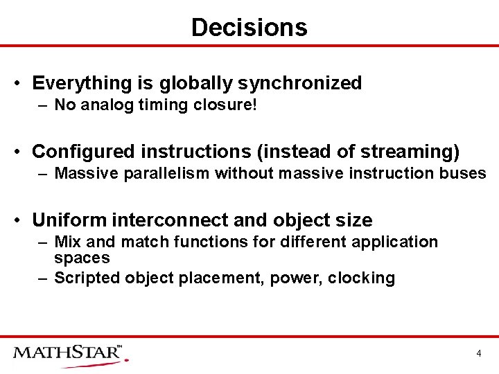
Decisions • Everything is globally synchronized – No analog timing closure! • Configured instructions (instead of streaming) – Massive parallelism without massive instruction buses • Uniform interconnect and object size – Mix and match functions for different application spaces – Scripted object placement, power, clocking 4
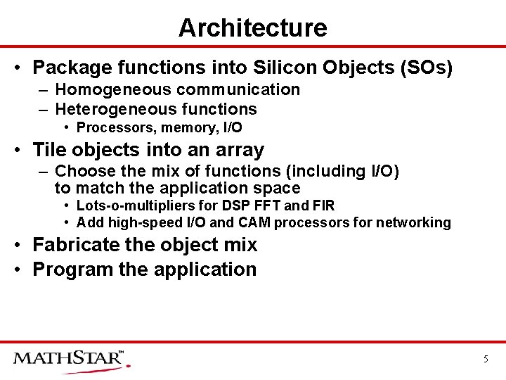
Architecture • Package functions into Silicon Objects (SOs) – Homogeneous communication – Heterogeneous functions • Processors, memory, I/O • Tile objects into an array – Choose the mix of functions (including I/O) to match the application space • Lots-o-multipliers for DSP FFT and FIR • Add high-speed I/O and CAM processors for networking • Fabricate the object mix • Program the application 5
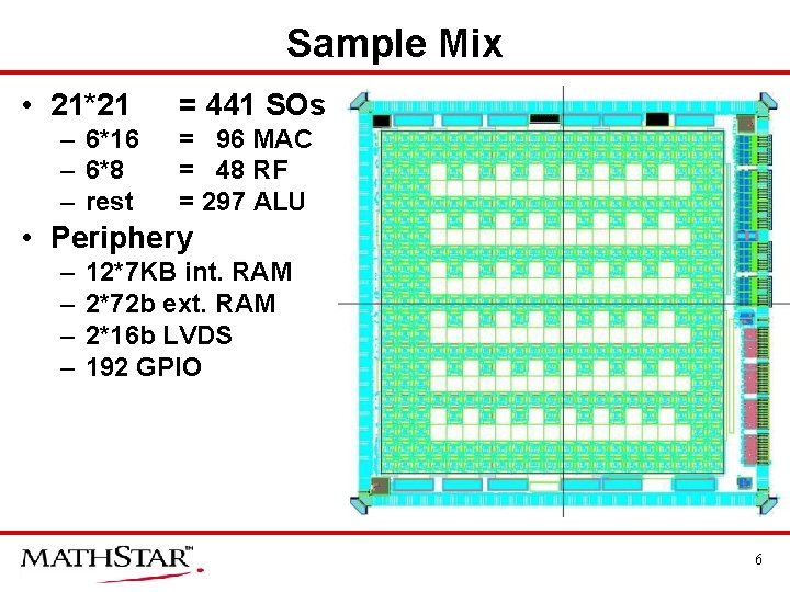
Sample Mix • 21*21 – 6*16 – 6*8 – rest = 441 SOs = 96 MAC = 48 RF = 297 ALU • Periphery – – 12*7 KB int. RAM 2*72 b ext. RAM 2*16 b LVDS 192 GPIO 6
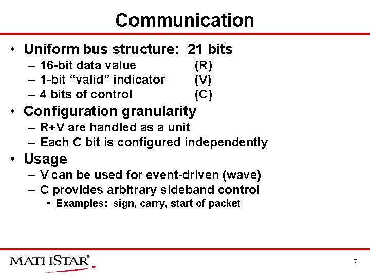
Communication • Uniform bus structure: 21 bits – 16 -bit data value – 1 -bit “valid” indicator – 4 bits of control (R) (V) (C) • Configuration granularity – R+V are handled as a unit – Each C bit is configured independently • Usage – V can be used for event-driven (wave) – C provides arbitrary sideband control • Examples: sign, carry, start of packet 7
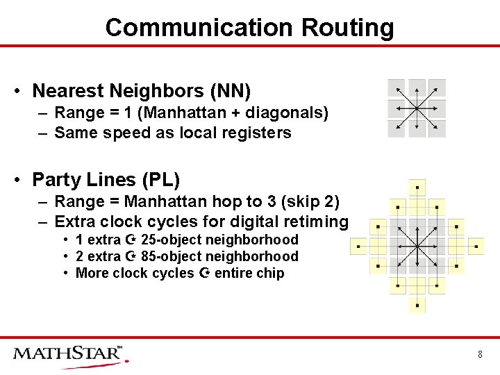
Communication Routing • Nearest Neighbors (NN) – Range = 1 (Manhattan + diagonals) – Same speed as local registers • Party Lines (PL) – Range = Manhattan hop to 3 (skip 2) – Extra clock cycles for digital retiming • 1 extra 25 -object neighborhood • 2 extra 85 -object neighborhood • More clock cycles entire chip 8
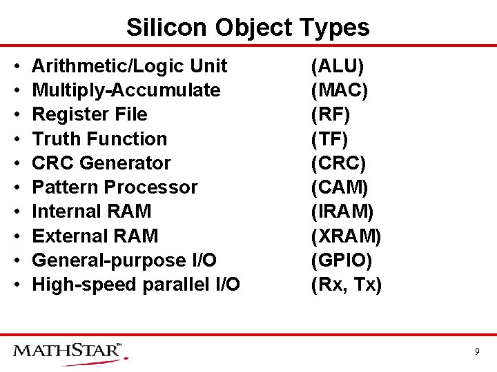
Silicon Object Types • • • Arithmetic/Logic Unit Multiply-Accumulate Register File Truth Function CRC Generator Pattern Processor Internal RAM External RAM General-purpose I/O High-speed parallel I/O (ALU) (MAC) (RF) (TF) (CRC) (CAM) (IRAM) (XRAM) (GPIO) (Rx, Tx) 9
Object Type: ALU 10
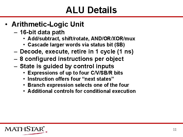
ALU Details • Arithmetic-Logic Unit – 16 -bit data path • Add/subtract, shift/rotate, AND/OR/XOR/mux • Cascade larger words via status bit (SB) – Decode, execute, retire in 1 cycle (1 ns) – 8 configured instructions per object – State is guided by control inputs • • Expressions of up to four C/V/SB/R bits Instruction offers four “next states” Branch expression selects one of the four Additional controls for conditional execution 11
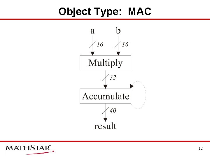
Object Type: MAC 12
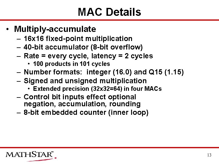
MAC Details • Multiply-accumulate – 16 x 16 fixed-point multiplication – 40 -bit accumulator (8 -bit overflow) – Rate = every cycle, latency = 2 cycles • 100 products in 101 cycles – Number formats: integer (16. 0) and Q 15 (1. 15) – Signed and unsigned multiplication • Extended precision (32 x 32=64) in four MACs – Control bit inputs effect optional negation, accumulation, rounding – 8 -bit embedded counter (inner loop) 13
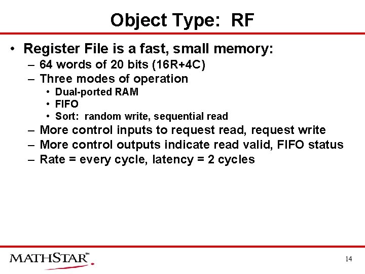
Object Type: RF • Register File is a fast, small memory: – 64 words of 20 bits (16 R+4 C) – Three modes of operation • Dual-ported RAM • FIFO • Sort: random write, sequential read – More control inputs to request read, request write – More control outputs indicate read valid, FIFO status – Rate = every cycle, latency = 2 cycles 14
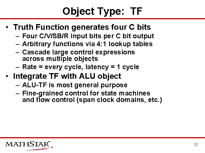
Object Type: TF • Truth Function generates four C bits – Four C/V/SB/R input bits per C bit output – Arbitrary functions via 4: 1 lookup tables – Cascade large control expressions across multiple objects – Rate = every cycle, latency = 1 cycle • Integrate TF with ALU object – ALU-TF is most general purpose – Fine-grained control for state machines and flow control (span clock domains, etc. ) 15
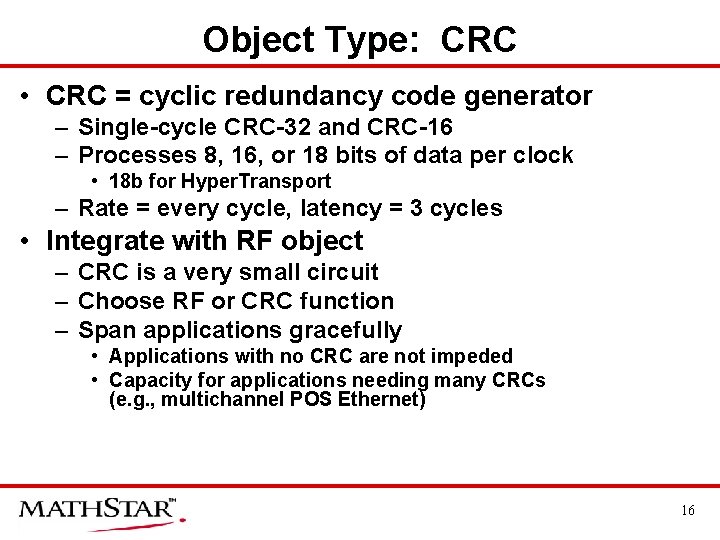
Object Type: CRC • CRC = cyclic redundancy code generator – Single-cycle CRC-32 and CRC-16 – Processes 8, 16, or 18 bits of data per clock • 18 b for Hyper. Transport – Rate = every cycle, latency = 3 cycles • Integrate with RF object – CRC is a very small circuit – Choose RF or CRC function – Span applications gracefully • Applications with no CRC are not impeded • Capacity for applications needing many CRCs (e. g. , multichannel POS Ethernet) 16
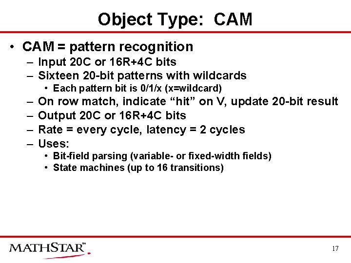
Object Type: CAM • CAM = pattern recognition – Input 20 C or 16 R+4 C bits – Sixteen 20 -bit patterns with wildcards • Each pattern bit is 0/1/x (x=wildcard) – – On row match, indicate “hit” on V, update 20 -bit result Output 20 C or 16 R+4 C bits Rate = every cycle, latency = 2 cycles Uses: • Bit-field parsing (variable- or fixed-width fields) • State machines (up to 16 transitions) 17
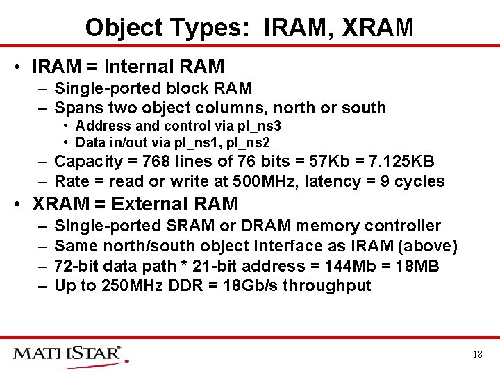
Object Types: IRAM, XRAM • IRAM = Internal RAM – Single-ported block RAM – Spans two object columns, north or south • Address and control via pl_ns 3 • Data in/out via pl_ns 1, pl_ns 2 – Capacity = 768 lines of 76 bits = 57 Kb = 7. 125 KB – Rate = read or write at 500 MHz, latency = 9 cycles • XRAM = External RAM – – Single-ported SRAM or DRAM memory controller Same north/south object interface as IRAM (above) 72 -bit data path * 21 -bit address = 144 Mb = 18 MB Up to 250 MHz DDR = 18 Gb/s throughput 18
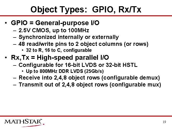
Object Types: GPIO, Rx/Tx • GPIO = General-purpose I/O – 2. 5 V CMOS, up to 100 MHz – Synchronized internally or externally – 48 read/write pins to 2 object columns (or rows) • 32 to R, 16 to C, configurable • Rx, Tx = High-speed parallel I/O – Configurable for 16 -bit LVDS or 32 -bit HSTL • Up to 800 MHz DDR LVDS (25 Gb/s) – Receive into 2, 4, 8 object rows (configurable demux) – Transmit out of 2, 4, 8 object rows (configurable mux) 19
DSP Algorithms in Objects • • Complex Multiplication Radix-2 DIT Butterfly Radix-4 DIF Dragonfly Fast Fourier Transform (FFT) 20
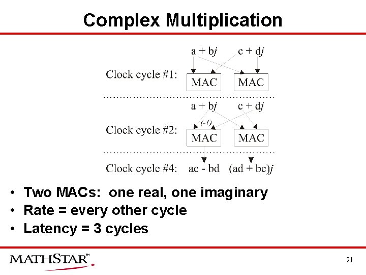
Complex Multiplication • Two MACs: one real, one imaginary • Rate = every other cycle • Latency = 3 cycles 21
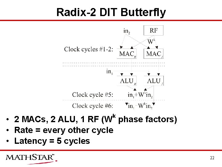
Radix-2 DIT Butterfly • 2 MACs, 2 ALU, 1 RF (Wk phase factors) • Rate = every other cycle • Latency = 5 cycles 22
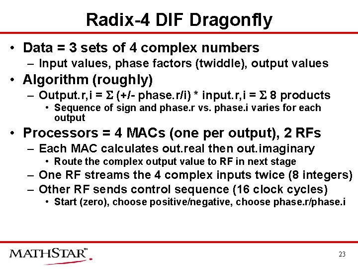
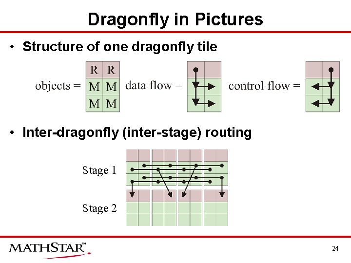
Radix-4 DIF Dragonfly • Data = 3 sets of 4 complex numbers – Input values, phase factors (twiddle), output values • Algorithm (roughly) – Output. r, i = (+/- phase. r/i) * input. r, i = 8 products • Sequence of sign and phase. r vs. phase. i varies for each output • Processors = 4 MACs (one per output), 2 RFs – Each MAC calculates out. real then out. imaginary • Route the complex output value to RF in next stage – One RF streams the 4 complex inputs twice (8 integers) – Other RF sends control sequence (16 clock cycles) • Start (zero), choose positive/negative, choose phase. r/phase. i 23
Dragonfly in Pictures • Structure of one dragonfly tile • Inter-dragonfly (inter-stage) routing Stage 1 Stage 2 24
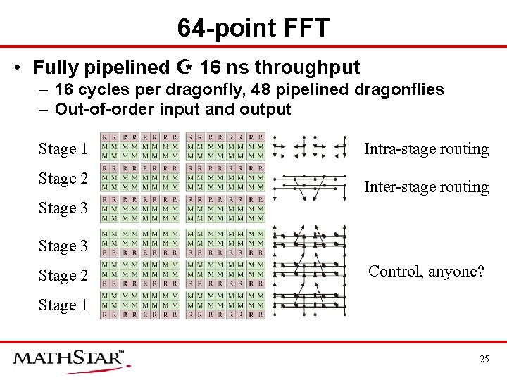
64 -point FFT • Fully pipelined 16 ns throughput – 16 cycles per dragonfly, 48 pipelined dragonflies – Out-of-order input and output Stage 1 Intra-stage routing Stage 2 Inter-stage routing Stage 3 Stage 2 Control, anyone? Stage 1 25
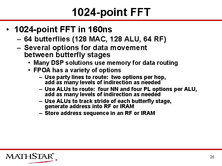
1024 -point FFT • 1024 -point FFT in 160 ns – 64 butterflies (128 MAC, 128 ALU, 64 RF) – Several options for data movement between butterfly stages • Many DSP solutions use memory for data routing • FPOA has a variety of options – Use party lines to route: two options per hop, add as many levels of indirection as needed – Use ALUs to route: four NN and four PL options per ALU, add as many levels of indirection as needed – Use ALUs to track stride of each butterfly stage, generate address into RF or IRAM – Store address sequence in an RF or IRAM 26
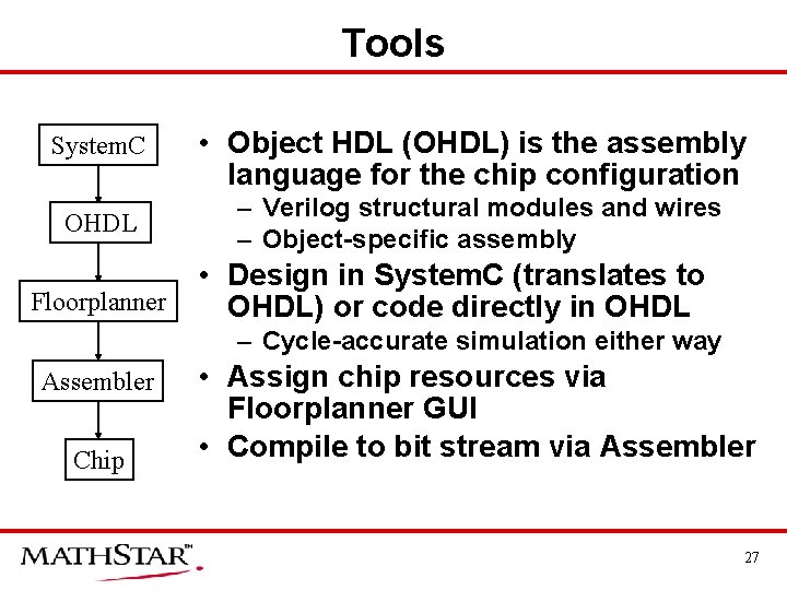
Tools System. C • Object HDL (OHDL) is the assembly language for the chip configuration OHDL – Verilog structural modules and wires – Object-specific assembly Floorplanner • Design in System. C (translates to OHDL) or code directly in OHDL – Cycle-accurate simulation either way Assembler Chip • Assign chip resources via Floorplanner GUI • Compile to bit stream via Assembler 27
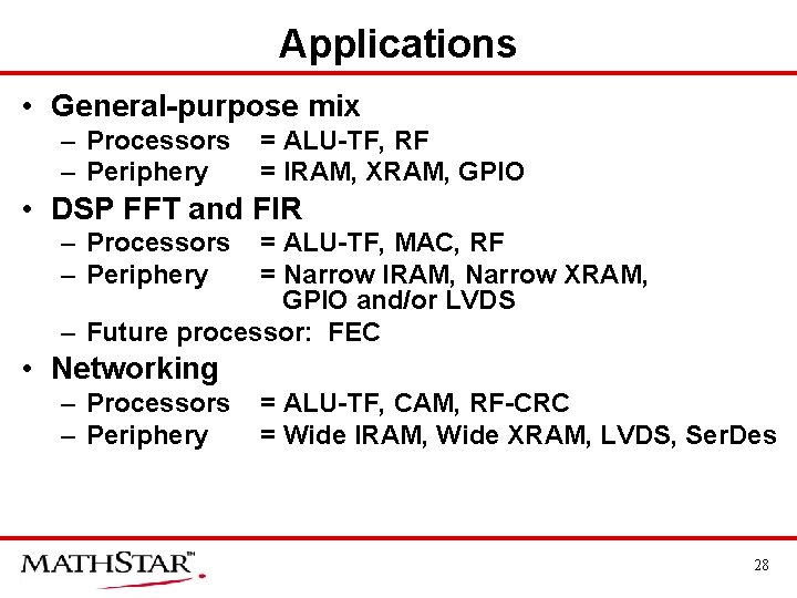
Applications • General-purpose mix – Processors – Periphery = ALU-TF, RF = IRAM, XRAM, GPIO • DSP FFT and FIR – Processors – Periphery = ALU-TF, MAC, RF = Narrow IRAM, Narrow XRAM, GPIO and/or LVDS – Future processor: FEC • Networking – Processors – Periphery = ALU-TF, CAM, RF-CRC = Wide IRAM, Wide XRAM, LVDS, Ser. Des 28
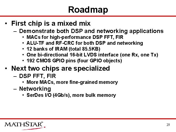
Roadmap • First chip is a mixed mix – Demonstrate both DSP and networking applications • • • MACs for high-performance DSP FFT, FIR ALU-TF and RF-CRC for both DSP and networking 12 banks of IRAM (total 85. 5 KB) One bi-directional 16 -bit LVDS interface (one Rx, one Tx) 192 CMOS GPIO pins (four GPIO objects) • Next two chips are specialized – DSP FFT, FIR • More MACs, more fine-grained memory – Networking • Ser. Des I/O (4 Gb/s), more bulk memory 29
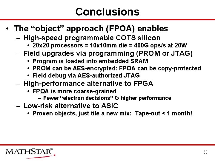
Conclusions • The “object” approach (FPOA) enables – High-speed programmable COTS silicon • 20 x 20 processors = 10 x 10 mm die = 400 G ops/s at 20 W – Field upgrades via programming (PROM or JTAG) • Program is loaded into embedded SRAM • PROM can be AES-encrypted; FPOA can be copy-protected • Field debug via AES-authorized JTAG – High-performance alternative to FPGA • FPOA is more coarse-grained – Fewer “electron decisions” higher performance – Low-risk alternative to ASIC • Proven objects, just tile a new mix: Tape-out < 1 month! 30