Denso TPS 54160 Q 1 low dropout operation

- Slides: 13

Denso TPS 54160 -Q 1 “low dropout” operation Todd Toporski Analog Field Applications 2/4/2011 1

TPS 54160 -Q 1 Overview • • • Buck circuit recommended to Denso Description of “low dropout” operation What “low dropout” condition looks like Work-around used by Denso-Japan TI recommendations 2

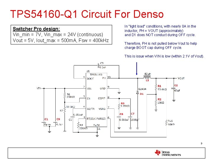
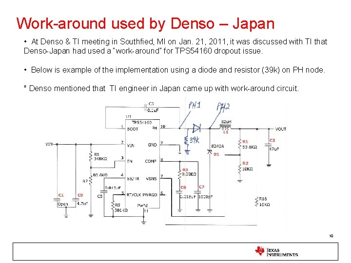
TPS 54160 -Q 1 Circuit For Denso Switcher Pro design: Vin_min = 7 V, Vin_max = 24 V (continuous) Vout = 5 V, Iout_max = 500 m. A, Fsw = 400 k. Hz In “light load” conditions, with nearly 0 A in the inductor, PH = VOUT (approximately) and D 1 does NOT conduct during OFF cycle. Therefore, PH is not pulled below Vout to help charge BOOT cap during OFF cycle. This is issue when VIN is low (within 2. 1 V of Vout). 3

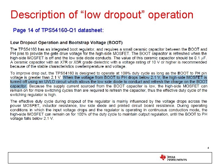
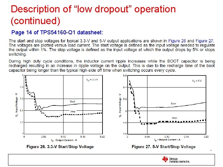
Description of “low dropout” operation Page 14 of TPS 54160 -Q 1 datasheet: 4

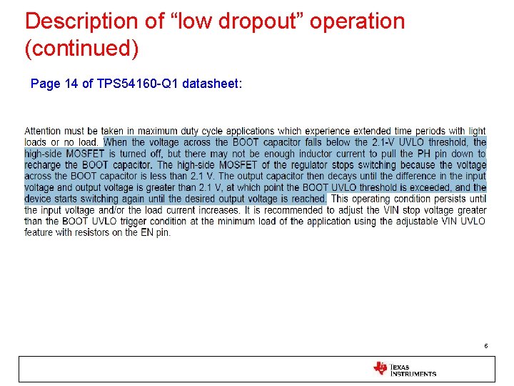
Description of “low dropout” operation (continued) Page 14 of TPS 54160 -Q 1 datasheet: 5

Description of “low dropout” operation (continued) Page 14 of TPS 54160 -Q 1 datasheet: 6

Description of “low dropout” operation (continued) • To reduce power consumption in light load conditions, TPS 54160 -Q 1 uses a BOOTSTRAP circuit for driving the gate of the internal highside FET. • Another method to supply gate voltage for driving internal highside FET is to use a CHARGE PUMP. • Disadvantage of CHARGE PUMP is it requires clock and consumes more quiescent current. Advantage of BOOTSTRAP is it does not require a clock, and it consumes less quiescent current. • Advantage of CHARGE PUMP is it provides better FET drive in “low dropout” conditions. Disadvantage of BOOTSTRAP is it can be problematic in “low dropout” conditions for driving the FET. • The BOOTSTRAP & “low dropout” limitation experienced on TPS 54160 -Q 1 is similarly experienced on other buck switchers using BOOTSTRAP. 7

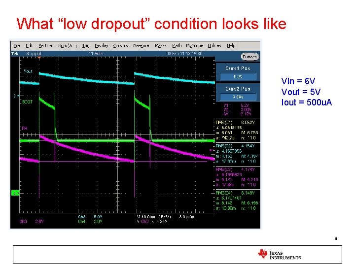
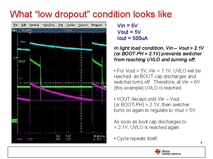
What “low dropout” condition looks like Vin = 6 V Vout = 5 V Iout = 500 u. A 8

What “low dropout” condition looks like Vin = 6 V Vout = 5 V Iout = 500 u. A In light load condition, Vin – Vout > 2. 1 V (or BOOT-PH > 2. 1 V) prevents switcher from reaching UVLO and turning off. • For Vout = 5 V, Vin < 7. 1 V, UVLO will be reached as BOOT cap discharges and switcher turns off. Therefore, at Vin = 6 V (this example) UVLO is reached. • VOUT decays until Vin – Vout (or BOOT-PH) > 2. 1 V, then switcher turns on again to regulate to Vout = 5 V. As soon as boot cap discharges to < 2. 1 V, UVLO is reached again. • Cycle repeats itself. 9

Work-around used by Denso – Japan • At Denso & TI meeting in Southfied, MI on Jan. 21, 2011, it was discussed with TI that Denso-Japan had used a “work-around” for TPS 54160 dropout issue. • Below is example of the implementation using a diode and resistor (39 k) on PH node. * Denso mentioned that TI engineer in Japan came up with work-around circuit. 10

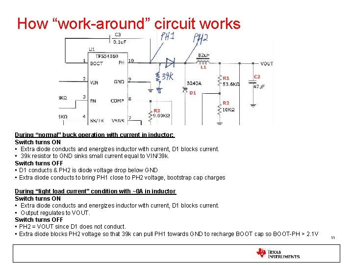
How “work-around” circuit works During “normal” buck operation with current in inductor: Switch turns ON • Extra diode conducts and energizes inductor with current, D 1 blocks current. • 39 k resistor to GND sinks small current equal to VIN/39 k. Switch turns OFF • D 1 conducts & PH 2 is diode voltage drop below GND • Extra diode conducts to bring PH 1 close to PH 2 voltage, bootstrap charges During “light load current” condition with ~0 A in inductor Switch turns ON • Extra diode conducts and energizes inductor with current, D 1 blocks current. • Output regulates to VOUT. Switch turns OFF • PH 2 = VOUT since D 1 does not conduct. • Extra diode blocks PH 2 voltage so that 39 k can pull PH 1 towards GND to recharge BOOT cap so BOOT-PH > 2. 1 V 11

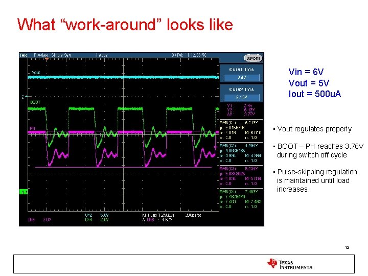
What “work-around” looks like Vin = 6 V Vout = 5 V Iout = 500 u. A • Vout regulates properly • BOOT – PH reaches 3. 76 V during switch off cycle • Pulse-skipping regulation is maintained until load increases. 12

TI Recommendations & Summary • Work-around circuit appears to work for helping dropout condition, but should be tested over all conditions deemed necessary by Denso. • Drawback of “work-around” circuit is it dissipates more losses (across diode) when load current increases. For 500 m. A application these losses are not very large. • For larger load currents, such as 1 A or higher, the “work-around” circuit will dissipate more power across the diode and this should be accounted for in the design. 13