Decapsulation method for multichip MCP devices YEAP MING
 devices • YEAP MING HONG • TEH AI XUAN")


? � MCP refers to a packaging configuration containing not more")


 decapsulation is now becoming a rising problem. Because for traditional")

- Slides: 17
Decapsulation method for multichip (MCP) devices • YEAP MING HONG • TEH AI XUAN • CHIN SHIK YI • HUSNA BINTI MOHD YUSOF • NOR ROSSAMA BINTI IBRAHIM 101011378 101011281 101011479 101010302 101010851
INTRODUCTION
WHAT IS DE-CAPSULATION? Decapsulation is the removal of a cap, lid, or encapsulating material from a packaged integrated circuit by mechanical, thermal, or chemical means. Decapsulation exposes the integrated circuit for the purpose of further analysis. It is physically destructive and the process leaves the die, bond pads and wire bonds intact.
WHY PERFORM DECAPSULATION? �Decapsulation is performed to gain access to the package cavity and/or surface of a device for the purpose of further analysis. �In the case of a hermetic device, removal of the lid permits visual inspection foreign material, corrosion, mechanical damage, or other workmanship and processing issues. Removal of polymeric encapsulating material from a plastic packaged part also reveals the IC surface. It allows FA techniques--such as high resolution optical microscopy, electrical probing, and electron beam-- to become possible and opens the door for removal and deprocessing of the IC.
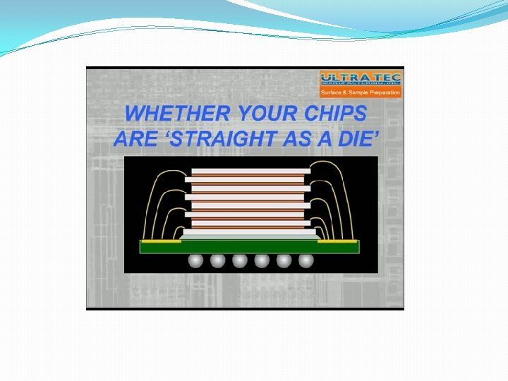
WHAT IS MULTICHIP PACKAGE(MCP)? � MCP refers to a packaging configuration containing not more than five (5) chips, connected via wire bonds to a multilayer circuit board, and protected by either a molded encapsulant or a low-cost ceramic package. � In the simplest case, dies can be attached to a die paddle without a substrate, and inter-die communication is achieved through die-to-die wire bonding.
HOW? � For performing failure analysis on the MCP devices, the package decapsulation performed using a commercial chemical automatic jet-etch de-capper (auto-decapper). � First of all, the top die will be removed without employing a wet chemical etch, next, the residual attach and package material of the bottom die of the multichip device will be removed. � First method will demonstrate decapsulation by using mechanical polishing for the first die and dry etching to expose second die. Second method will demonstrate decapsulation using mechanical polishing for the first die and wet etching to expose second die. Third method is fully mechanical decapsulation by using ASAP -1 machinery. � If the failure analysis is required on the bottom die, this technique is challenge to remove the top die while keeping the bottom die fully functional for further analysis. � Accordingly, the decapsulation technique should able to removed a top die without damaging the bottom die in a multi-chip package in order to retain full failure analysis capability on these types of packaged devices.
PRINCIPLE
METHOD 1 : PLASMA DRY ETCHING PROCESS 1. Polish off package connectors 2. Polish off top die Expose the bottom die with plasma ecth 3. First polishing step to polish off circuit connection material, e. g. solder balls, on the backside of the package. (improves the uniformity of polishing for the top die removal. ) - 30 um polish sheet for 20 minutes in high precision polisher. Remounting the device in a sample holder and perform second polishing step to remove the top die The second polishing step suitably uses: - 30 um polish sheet for 20 minutes - to remove most of the top die(10) until the adhesive(12) layer between the die 1 and die 2 show at a corner. - then, 3 um polish sheet for 30 minutes to remove the remaining top die silicon and expose the entire adhesive/polyimide(12) layer on top and bottom die(14) Once the top die is removed, the process continues with removal of the remaining adhesive/polyimide(12) layer and plastic compound in the bond pad areas of the bottom die(14) through plasma dry etching. - Plasma dry etch: use of an oxygen/argon plasma chemical - Plasma power : 150 W (watts), - Plasma flow : 20 milli. Torr - Plasma etching time: 20 -40 minutes (until all bond pads are exposed)
ADVANTAGES � No wet chemical etching is involved through the entire top die removal process. Thus, the bottom die is unlikely to be damaged due to wet chemical exposure. � Uniformity of polishing is important for the success, since the polishing process needs to stop at the adhesive level between the two dies, which is only around 1 -2 um thick. DISADVANTAGES � While providing better avoidance of damage to the bottom die, it is unfortunate that the original package cannot be used for electrical testing, since all wire bonds are polished off during the process. In order to electrically test the device, the polished needs to be assembled in a new package, such as a Ceramic Dual-In-Line Package (CDIP), for further analysis.
METHOD 2 – CHEMICAL ETCHING PROCESS 1. Start with a polishing step. The polishing step partially polishes off the top die(10) using a high precision polisher. - 30 um polish sheet used for 15 minutes The polishing is stopped before reaching the highest point of the wire bond loops (24) of the bottom die. 2. A chemical etching step to etch off the remaining part of the top die follows by immersing the entire package in an appropriate chemical solution. -chemical etch conditions include the use of KOH (potassium hydroxide 45%) as the etchant at an etch temperature of 110 -120° C for about 20 minutes or until the top die(10) is completely etched off. 3. Once the top die is removed, the entire bottom die is exposed by etching off the adhesive (12) via chemical decapsulation using an auto decapper -chemical decapsulation uses fuming sulfuric acid with an etch temperature of 200° C. , a heat-up time of about 120 seconds, an etch time of about 80 seconds, and a rinse time of about 22 seconds. Partially polish off top die Chemical etch top die Etch to expose the bottom die
ADVANTAGES �Ability to use the original package for electrical testing while providing for decapsulation to expose the bottom die. DISADVANTAGES �Chemical involved �Dangerous/ hazard
SAMPLE: FLASH MEMORY DIE AS A TOP DIE AND A STATIC RANDOM ACCESS MEMORY (SRAM) DIE AS A BOTTOM DIE
METHOD 3 – MECHANICAL DECAPSULATION �Device: ASAP-1 machinery �Multi-chip CSP’s provide an unique challenge to the failure analyst in that standard chemical decapsulation. Particularly if the package contains two or more stacked dice. ASAP-1 machinery allows for rapid and effective CSP decapsulation with resulting “live” circuitry for testing and failure analysis.
CONCLUSION
�Since multi-chip package (MCP) decapsulation is now becoming a rising problem. Because for traditional decapsulation method, acid can’t dissolve the top silicon die to expose the bottom die surface in MCP. It makes inspecting the bottom die in MCP is difficult. Thus, the new MCP decapsulation technology combining which combine mechanical polishing with chemical etching are introduced to solve this problem.
THANKYOU^^