Daniel Magalotti University of Modena and Reggio Emilia

- Slides: 20

Daniel Magalotti University of Modena and Reggio Emilia INFN of Perugia Software for tests: AMB and LAMB configuration - Available tools FTK Workshop – Pisa 13/03/2013

Outline � VME standard protocol description � AMBoard & LAMB configuration � AMchip configuration and control � Tools and software for testing 2 FTK Workshop 13/03/2013 Pisa - Daniel Magalotti

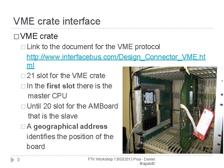
VME crate interface � VME crate � Link to the document for the VME protocol http: //www. interfacebus. com/Design_Connector_VME. ht ml � 21 slot for the VME crate � In the first slot there is the master CPU � Until 20 slot for the AMBoard that is the slave � A geographical address identifies the position of the board 3 FTK Workshop 13/03/2013 Pisa - Daniel Magalotti

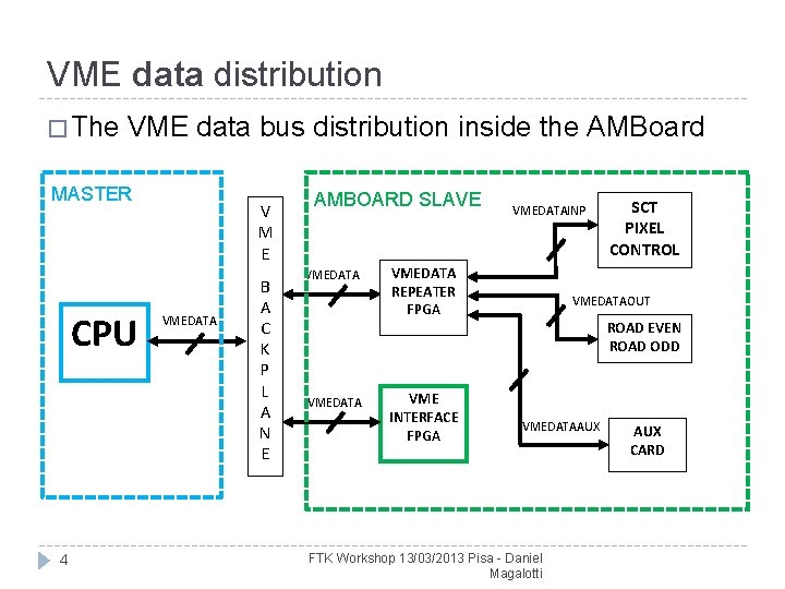
VME data distribution � The VME data bus distribution inside the AMBoard MASTER CPU 4 V M E VMEDATA B A C K P L A N E AMBOARD SLAVE VMEDATAINP VMEDATA REPEATER FPGA VME INTERFACE FPGA SCT PIXEL CONTROL VMEDATAOUT ROAD EVEN ROAD ODD VMEDATAAUX FTK Workshop 13/03/2013 Pisa - Daniel Magalotti AUX CARD

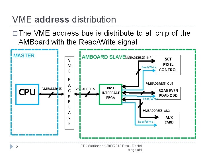
VME address distribution � The VME address bus is distribute to all chip of the AMBoard with the Read/Write signal MASTER CPU 5 V M E VMEADDRESS B A C K P L A N E AMBOARD SLAVEVMEADDRESS_INP Read/Write VMEADDRESS SCT PIXEL CONTROL VMEADDRESS_OUT VME INTERFACE FPGA Read/Write ROAD EVEN ROAD ODD VMEADDRESS_AUX Read/Write FTK Workshop 13/03/2013 Pisa - Daniel Magalotti AUX CARD

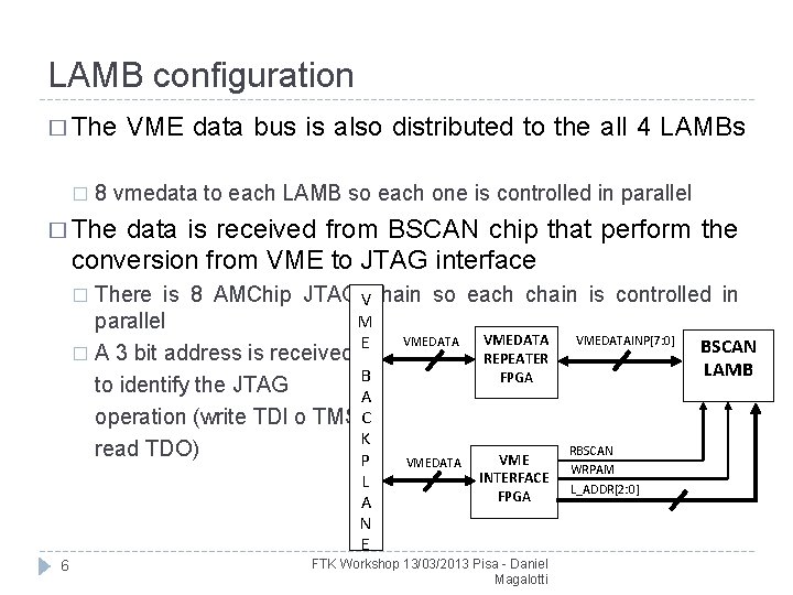
LAMB configuration � The VME data bus is also distributed to the all 4 LAMBs � 8 vmedata to each LAMB so each one is controlled in parallel � The data is received from BSCAN chip that perform the conversion from VME to JTAG interface There is 8 AMChip JTAG Vchain so each chain is controlled in M parallel VMEDATAINP[7: 0] VMEDATA E BSCAN � A 3 bit address is received REPEATER LAMB B FPGA to identify the JTAG A operation (write TDI o TMS C K RBSCAN read TDO) VME P � L A N E 6 VMEDATA INTERFACE FPGA FTK Workshop 13/03/2013 Pisa - Daniel Magalotti WRPAM L_ADDR[2: 0]

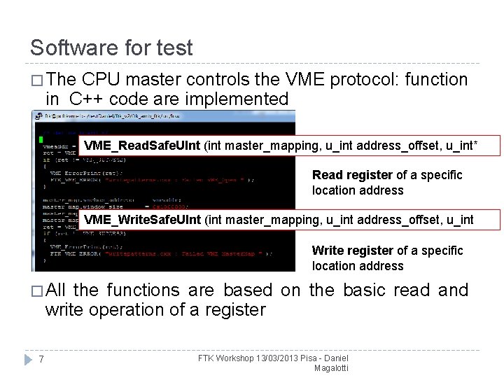
Software for test � The CPU master controls the VME protocol: function in C++ code are implemented VME_Read. Safe. UInt (int master_mapping, u_int address_offset, u_int* value); Read register of a specific location address VME_Write. Safe. UInt (int master_mapping, u_int address_offset, u_int value); Write register of a specific location address � All the functions are based on the basic read and write operation of a register 7 FTK Workshop 13/03/2013 Pisa - Daniel Magalotti

Software for test � The principal operations with the software � Configure and control the AMchips � Testing the hardware connection to/from AMchips with JTAG standard � Readout of the Spy. Buffer and writing of Vme. Fifo � Automatic script to testing the entire system 8 FTK Workshop 13/03/2013 Pisa - Daniel Magalotti

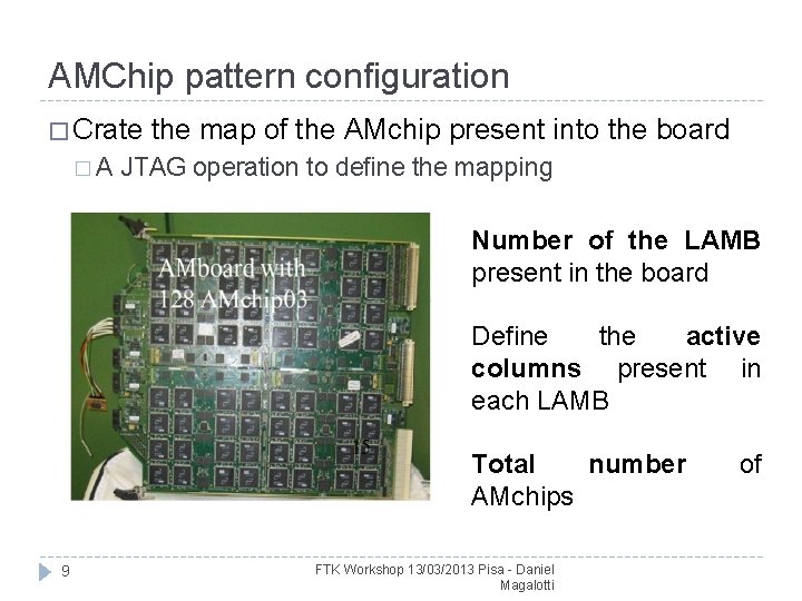
AMChip pattern configuration � Crate the map of the AMchip present into the board � A JTAG operation to define the mapping Number of the LAMB present in the board Define the active columns present in each LAMB Total number AMchips 9 FTK Workshop 13/03/2013 Pisa - Daniel Magalotti of

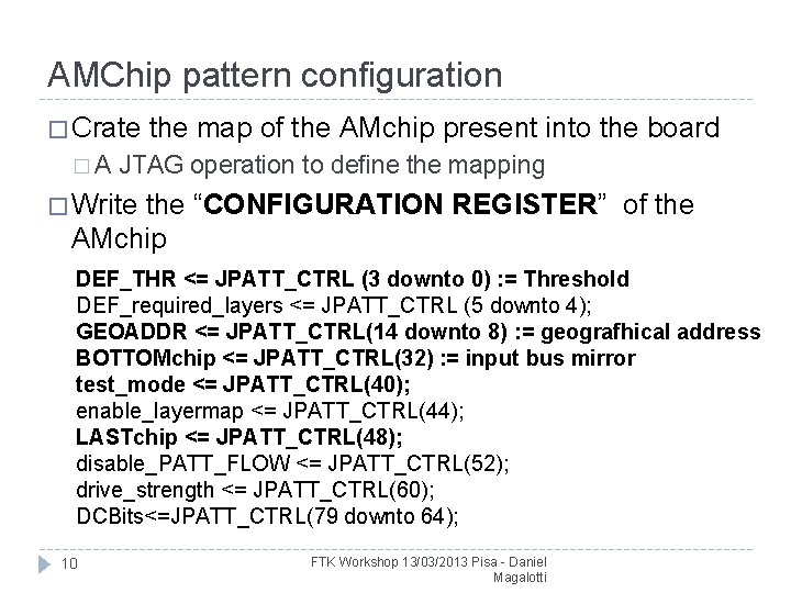
AMChip pattern configuration � Crate the map of the AMchip present into the board � A JTAG operation to define the mapping � Write the “CONFIGURATION REGISTER” of the AMchip DEF_THR <= JPATT_CTRL (3 downto 0) : = Threshold DEF_required_layers <= JPATT_CTRL (5 downto 4); GEOADDR <= JPATT_CTRL(14 downto 8) : = geografhical address BOTTOMchip <= JPATT_CTRL(32) : = input bus mirror test_mode <= JPATT_CTRL(40); enable_layermap <= JPATT_CTRL(44); LASTchip <= JPATT_CTRL(48); disable_PATT_FLOW <= JPATT_CTRL(52); drive_strength <= JPATT_CTRL(60); DCBits<=JPATT_CTRL(79 downto 64); 10 FTK Workshop 13/03/2013 Pisa - Daniel Magalotti

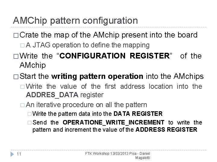
AMChip pattern configuration � Crate the map of the AMchip present into the board � A JTAG operation to define the mapping � Write the “CONFIGURATION REGISTER” of the AMchip � Start the writing pattern operation into the AMchips � Write the value of the first address location into the ADDRES_DATA register � An iterative procedure on all the pattern � Write the pattern data into the DATA REGISTER � Send the OPERATIONE_WRITE_INCREMENT to write the pattern and increment the value of the ADDRESS REGISTER 11 FTK Workshop 13/03/2013 Pisa - Daniel Magalotti

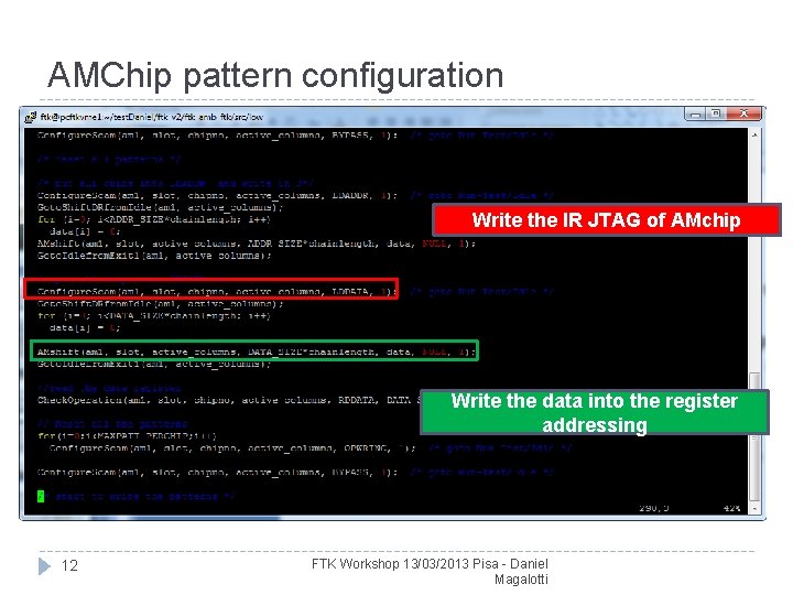
AMChip pattern configuration � Crate the map of the AMchip present into the board � A JTAG operation to define the mapping � Write the “CONFIGURATION Write REGISTER” of the IR JTAG of AMchip � Start the writing pattern operation into the AMchips � Write the value of the first address location into the ADDRES_DATA register � An iterative procedure on all the pattern Write the data into the register � Write the pattern data into the DATA REGISTER addressing � Send the OPERATIONE_WRITE_INCREMENT to write the pattern and increment the value of the ADDRESS REGISTER 12 FTK Workshop 13/03/2013 Pisa - Daniel Magalotti

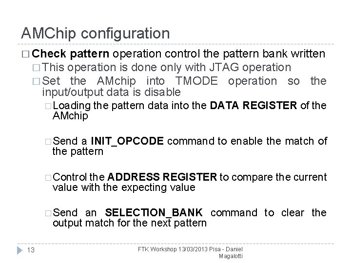
AMChip configuration � Check pattern operation control the pattern bank written � This operation is done only with JTAG operation � Set the AMchip into TMODE operation so the input/output data is disable � Loading the pattern data into the DATA AMchip � Send a INIT_OPCODE the pattern REGISTER of the command to enable the match of � Control the ADDRESS REGISTER to compare the current value with the expecting value � Send an SELECTION_BANK command to clear the output match for the next pattern 13 FTK Workshop 13/03/2013 Pisa - Daniel Magalotti

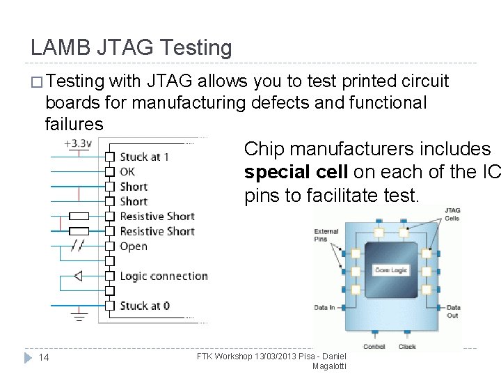
LAMB JTAG Testing � Testing with JTAG allows you to test printed circuit boards for manufacturing defects and functional failures 14 Chip manufacturers includes special cell on each of the IC pins to facilitate test. FTK Workshop 13/03/2013 Pisa - Daniel Magalotti

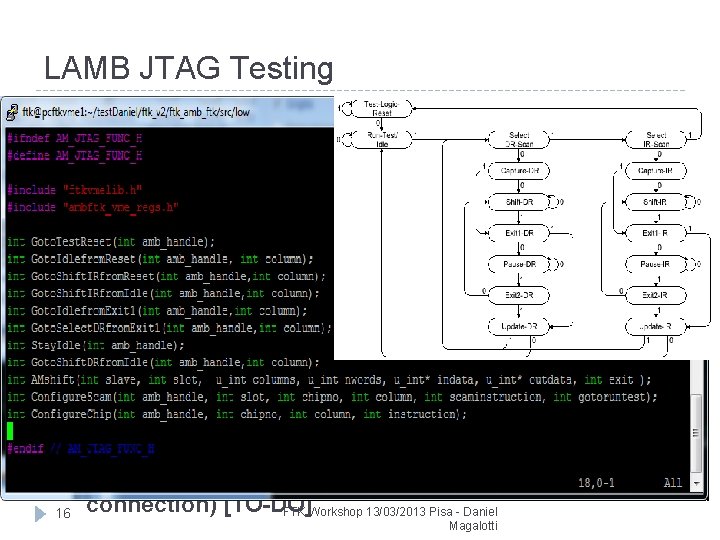
LAMB JTAG Testing � Testing with JTAG allows you to test printed circuit boards for manufacturing defects and functional failures � By driving signals between connected devices, nets can be tested for opens, shorts and stuck-at failures. � For testing all the pad of the AMchip we have to check � INput DIstributor to input pad of AMchips [DONE] � AMchips output to GLUE [TO-DO] � AMchips 15 output to AMchips input pad (pipeline connection) [TO-DO] FTK Workshop 13/03/2013 Pisa - Daniel Magalotti

LAMB JTAG Testing � Testing with JTAG allows you to test printed circuit boards for manufacturing defects and functional failures � By driving signals between connected devices, nets can be tested for opens, shorts and stuck-at failures. � For testing all the pad of the AMchip we have to check � INput DIstributor to input pad of AMchips [DONE] � AMchips output to GLUE [TO-DO] � AMchips 16 output to AMchips input pad (pipeline connection) [TO-DO] FTK Workshop 13/03/2013 Pisa - Daniel Magalotti

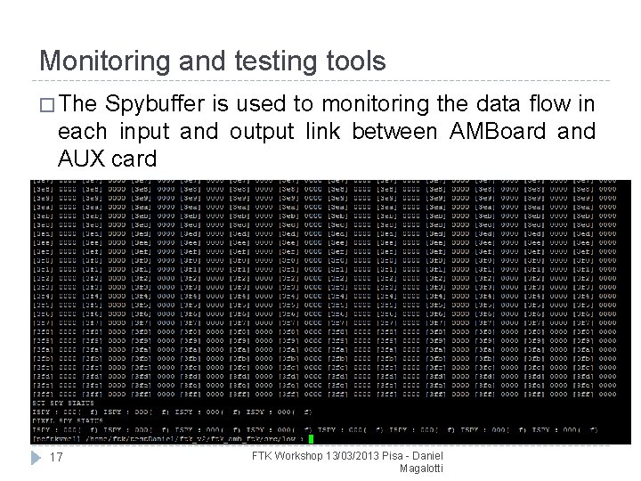
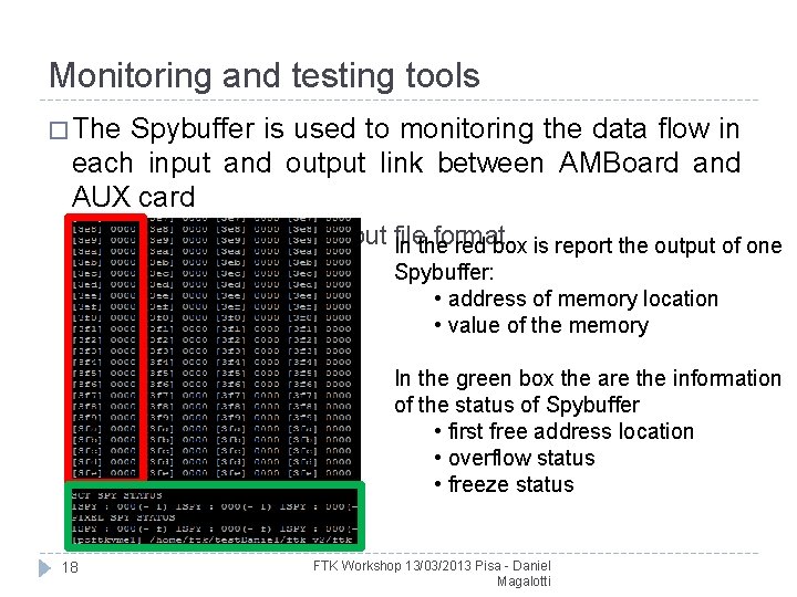
Monitoring and testing tools � The Spybuffer is used to monitoring the data flow in each input and output link between AMBoard and AUX card � A function give this output file format 17 FTK Workshop 13/03/2013 Pisa - Daniel Magalotti

Monitoring and testing tools � The Spybuffer is used to monitoring the data flow in each input and output link between AMBoard and AUX card � A function give this output file format In the red box is report the output of one Spybuffer: • address of memory location • value of the memory In the green box the are the information of the status of Spybuffer • first free address location • overflow status • freeze status 18 FTK Workshop 13/03/2013 Pisa - Daniel Magalotti

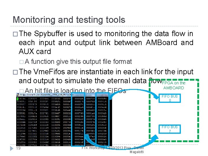
Monitoring and testing tools � The Spybuffer is used to monitoring the data flow in each input and output link between AMBoard and AUX card � A function give this output file format � The Vme. Fifos are instantiate in each link for the input and output to simulate the eternal data flow. FPGA on the � An hit file is loading into the FIFOs AMBOARD FIFO BUS 0 FIFO BUS 7 19 FTK Workshop 13/03/2013 Pisa - Daniel Magalotti

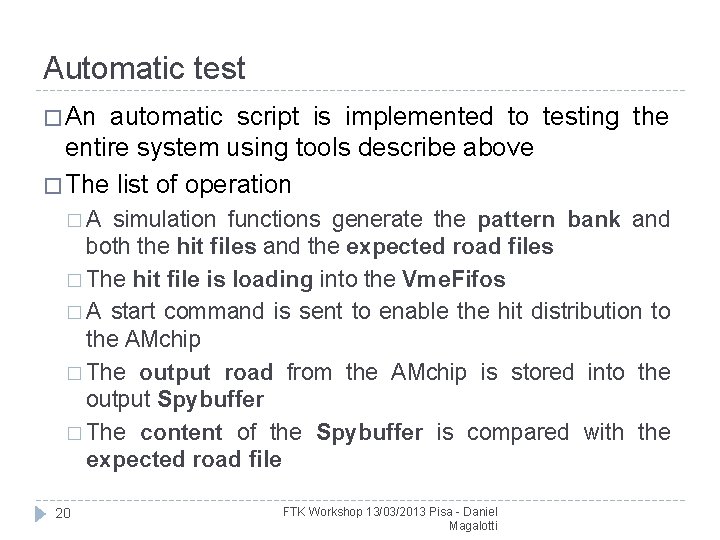
Automatic test � An automatic script is implemented to testing the entire system using tools describe above � The list of operation � A simulation functions generate the pattern bank and both the hit files and the expected road files � The hit file is loading into the Vme. Fifos � A start command is sent to enable the hit distribution to the AMchip � The output road from the AMchip is stored into the output Spybuffer � The content of the Spybuffer is compared with the expected road file 20 FTK Workshop 13/03/2013 Pisa - Daniel Magalotti