COMPERE Project Meeting Dr Dawei Xiang 03112008 Contents
![Simulation results (case 2: A↓) Fault detection based on gate voltage Monitoring [1] Simulated Simulation results (case 2: A↓) Fault detection based on gate voltage Monitoring [1] Simulated](https://slidetodoc.com/presentation_image_h2/b1f5930d5c79d3161b0a8bb84e56489e/image-13.jpg)


![Accelerated aging test Accelerated power cycling test system [5] It normally takes 2 -3 Accelerated aging test Accelerated power cycling test system [5] It normally takes 2 -3](https://slidetodoc.com/presentation_image_h2/b1f5930d5c79d3161b0a8bb84e56489e/image-28.jpg)

- Slides: 32

COMPERE Project Meeting Dr Dawei Xiang 03/11/2008

Contents I. IGBT terminal characteristics simulation II. VSI characteristic harmonics simulation III. Problems IV. Further work plan ESR Network

I. IGBT terminal characteristics simulation ESR Network

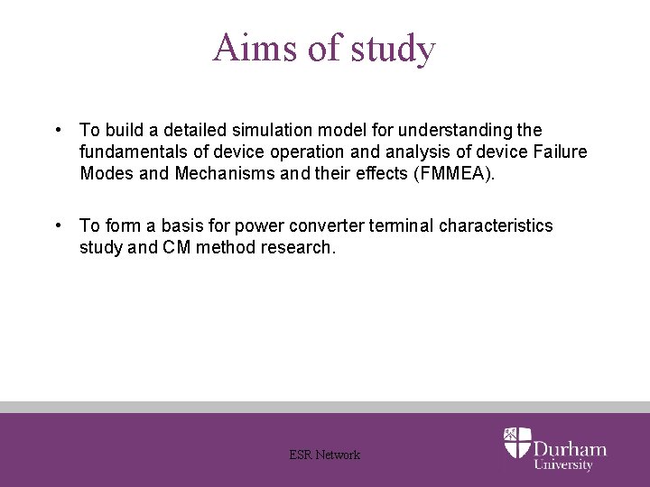
Aims of study • To build a detailed simulation model for understanding the fundamentals of device operation and analysis of device Failure Modes and Mechanisms and their effects (FMMEA). • To form a basis for power converter terminal characteristics study and CM method research. ESR Network

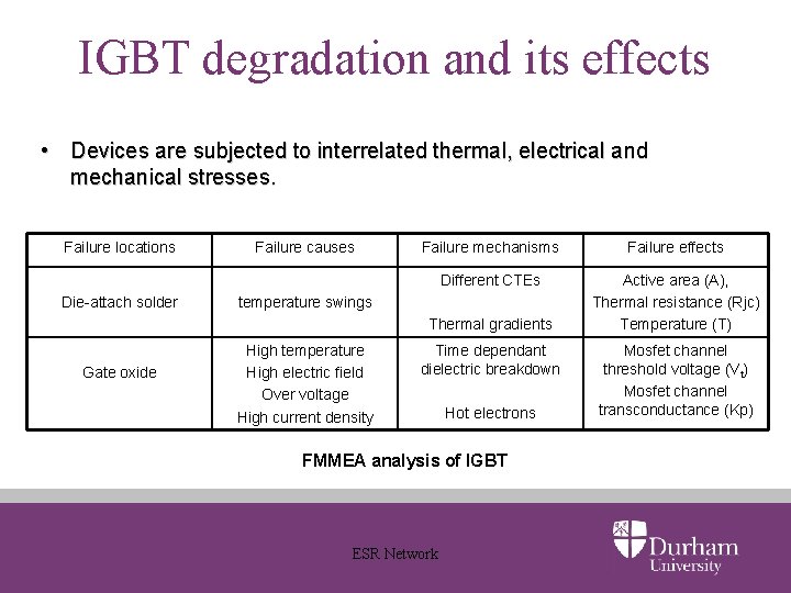
IGBT degradation and its effects • Devices are subjected to interrelated thermal, electrical and mechanical stresses. Failure locations Die-attach solder Failure causes Failure mechanisms Failure effects Different CTEs Active area (A), Thermal resistance (Rjc) Temperature (T) temperature swings Thermal gradients Gate oxide High temperature High electric field Over voltage High current density Time dependant dielectric breakdown Hot electrons FMMEA analysis of IGBT ESR Network Mosfet channel threshold voltage (Vt) Mosfet channel transconductance (Kp)

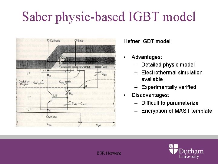
Saber physic-based IGBT model Hefner IGBT model • • ESR Network Advantages: – Detailed physic model – Electrothermal simulation available – Experimentally verified Disadvantages: – Difficult to parameterize – Encryption of MAST template

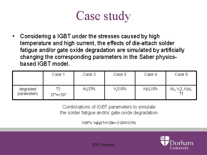
Case study • Considering a IGBT under the stresses caused by high temperature and high current, the effects of die-attach solder fatigue and/or gate oxide degradation are simulated by artificially changing the corresponding parameters in the Saber physicsbased IGBT model. degraded parameters Case 1 Case 2 Case 3 Case 4 Case 5 T↑: 27°=>50° A↓ 33% Vt↑ 10% Kp↓ 10% A↓, Vt↑, Kp↓, T↑ Combinations of IGBT parameters to simulate the solder fatigue and/or gate oxide degradation IGBTs: hgtg 27 n 120 bn (1200 V/27 A) ESR Network

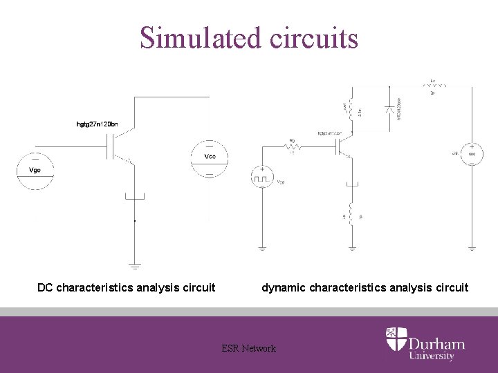
Simulated circuits DC characteristics analysis circuit dynamic characteristics analysis circuit ESR Network

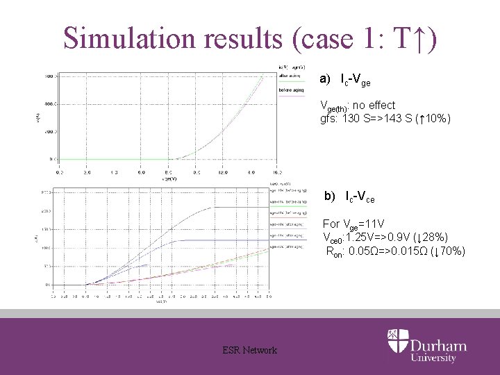
Simulation results (case 1: T↑) a) Ic-Vge Vge(th): no effect gfs: 130 S=>143 S (↑ 10%) b) Ic-Vce For Vge=11 V Vce 0: 1. 25 V=>0. 9 V (↓ 28%) Ron: 0. 05Ω=>0. 015Ω (↓ 70%) ESR Network

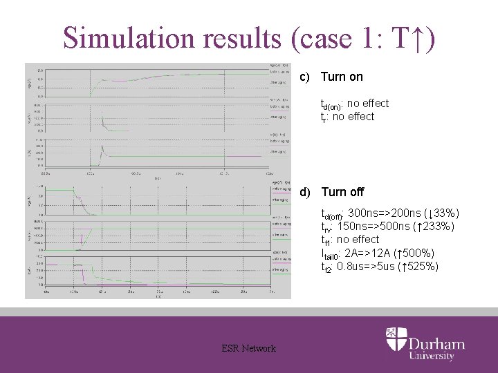
Simulation results (case 1: T↑) c) Turn on td(on): no effect tr: no effect d) Turn off td(off): 300 ns=>200 ns (↓ 33%) trv: 150 ns=>500 ns (↑ 233%) tf 1: no effect Itail 0: 2 A=>12 A (↑ 500%) tf 2: 0. 8 us=>5 us (↑ 525%) ESR Network

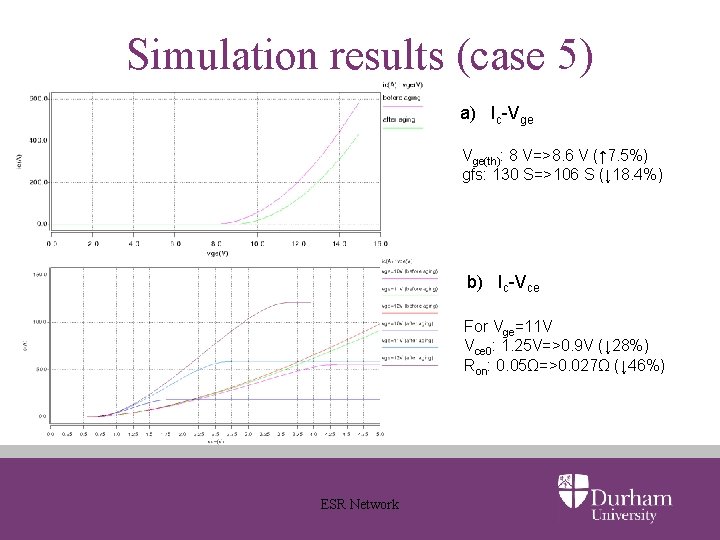
Simulation results (case 5) a) Ic-Vge Vge(th): 8 V=>8. 6 V (↑ 7. 5%) gfs: 130 S=>106 S (↓ 18. 4%) b) Ic-Vce For Vge=11 V Vce 0: 1. 25 V=>0. 9 V (↓ 28%) Ron: 0. 05Ω=>0. 027Ω (↓ 46%) ESR Network

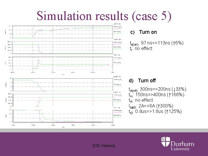
Simulation results (case 5) c) Turn on td(on): 97 ns=>113 ns (↑ 6%) tr: no effect d) Turn off td(off): 300 ns=>200 ns (↓ 33%) trv: 150 ns=>400 ns (↑ 166%) tf 1: no effect Itail 0: 2 A=>8 A (↑ 300%) tf 2: 0. 8 us=>1. 8 us (↑ 125%) ESR Network
![Simulation results case 2 A Fault detection based on gate voltage Monitoring 1 Simulated Simulation results (case 2: A↓) Fault detection based on gate voltage Monitoring [1] Simulated](https://slidetodoc.com/presentation_image_h2/b1f5930d5c79d3161b0a8bb84e56489e/image-13.jpg)
Simulation results (case 2: A↓) Fault detection based on gate voltage Monitoring [1] Simulated turn on transient [1] M. Rodriguez, A. Claudio, D. Theilliol et al. , “A new fault detection technique for IGBT based on gate voltage monitoring, ” in IEEE Power Electronics Specialists Conference, 17 -21 June 2007, pp. 1001 -1005. ESR Network

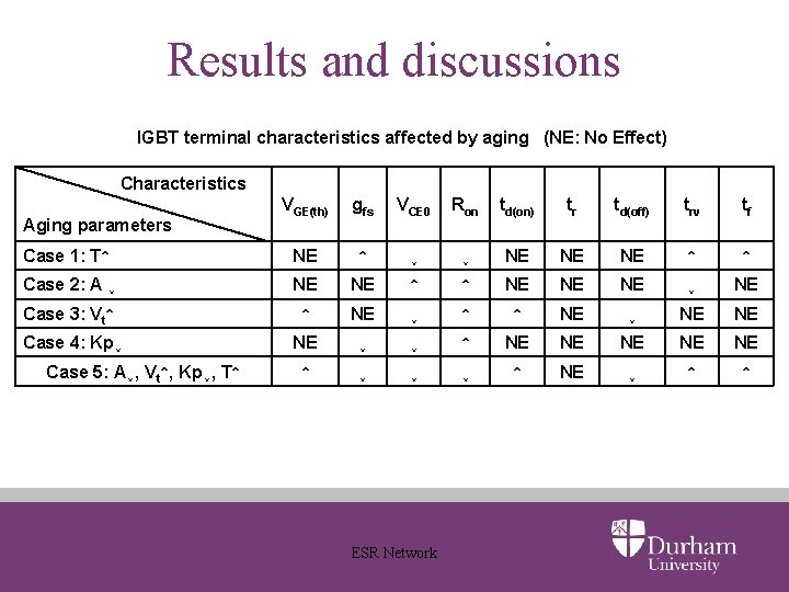
Results and discussions IGBT terminal characteristics affected by aging (NE: No Effect) Characteristics VGE(th) gfs VCE 0 Ron td(on) tr td(off) trv tf Case 1: T↑ NE ↑ ↓ ↓ NE NE NE ↑ ↑ Case 2: A ↓ NE NE ↑ ↑ NE NE NE ↓ NE Case 3: Vt↑ ↑ NE ↓ NE NE Case 4: Kp↓ NE ↓ ↓ ↑ NE NE NE ↑ ↓ ↓ ↓ ↑ NE ↓ ↑ ↑ Aging parameters Case 5: A↓, Vt↑, Kp↓, T↑ ESR Network

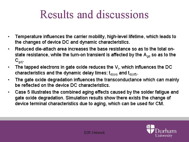
Results and discussions • • • Temperature influences the carrier mobility, high-level lifetime, which leads to the changes of device DC and dynamic characteristics. Reduced die-attach area increases the base resistance so as to the total onstate resistance, while the turn-on transient is affected by the Agd so as to the Cgdj. The tapped electrons in gate oxide reduces the Vt, which influences the DC characteristics and the dynamic delay times: td(on) and td(off). The gate oxide degradation influences the transconductance which can mainly be reflected on the device DC characteristics. Case 5 illustrates the combined aging effects caused by the solder fatigue and gate oxide degradation. Simulation results show there exists the change of device terminal characteristics due to aging, which can be used for CM. ESR Network

II. VSI characteristic harmonics simulation ESR Network

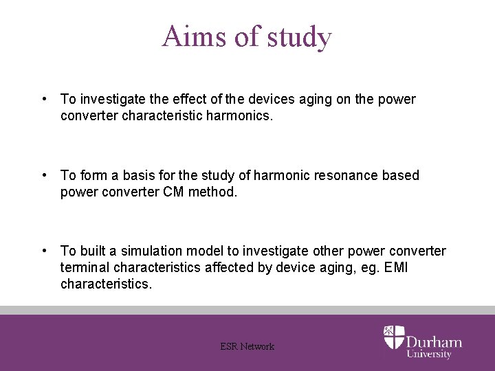
Aims of study • To investigate the effect of the devices aging on the power converter characteristic harmonics. • To form a basis for the study of harmonic resonance based power converter CM method. • To built a simulation model to investigate other power converter terminal characteristics affected by device aging, eg. EMI characteristics. ESR Network

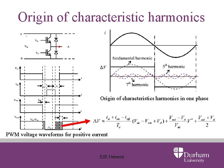
Origin of characteristic harmonics Origin of characteristics harmonics in one phase PWM voltage waveforms for positive current ESR Network

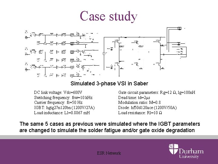
Case study Simulated 3 -phase VSI in Saber DC link voltage: Vdc=600 V Switching frequency: fsw=10 k. Hz Carrier frequency: fc=50 Hz IGBT: hgtg 27 n 120 bn (1200 V/27 A) Load inductance: Ll=0. 8867 m. H Gate circuit parameters: Rg=12 Ω, lg=100 n. H Dead time: td=2μs Modulation ratio: M=0. 8 Diode: hf 50 d 120 ace (1200 V/50 A) Load resistance: Rl=10 Ω The same 5 cases as previous were simulated where the IGBT parameters are changed to simulate the solder fatigue and/or gate oxide degradation ESR Network

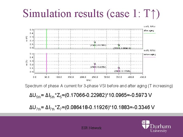
Simulation results (case 1: T↑) Spectrum of phase A current for 3 -phase VSI before and after aging (T increasing) ΔU 5 th= ΔI 5 th*Z 5=(0. 17066 -0. 22982)*10. 0965=-0. 5973 V ΔU 7 th= ΔI 7 th*Z 7=(0. 086418 -0. 11926)*10. 1883=-0. 3346 V ESR Network

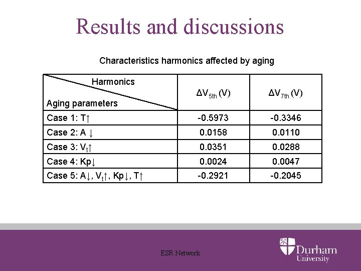
Results and discussions Characteristics harmonics affected by aging Harmonics ΔV 5 th (V) ΔV 7 th (V) Case 1: T↑ -0. 5973 -0. 3346 Case 2: A ↓ 0. 0158 0. 0110 Case 3: Vt↑ 0. 0351 0. 0288 Case 4: Kp↓ 0. 0024 0. 0047 Case 5: A↓, Vt↑, Kp↓, T↑ -0. 2921 -0. 2045 Aging parameters ESR Network

Results and discussions • The IGBT Vce 0 and switching behavior determines the amplitude of characteristic harmonics through changing the V-A characteristics of output PWM voltage during aging. • Simulation results show that characteristics harmonics are more sensitive to the changes of temperature while the other factors may have slight effects on them. • Under the predefined simulation conditions, a deviation of about 0. 3 V can be reached for 5 th harmonic. Such a variation falls in the range where our previous harmonic resonance method is capable of detecting. ESR Network

III. Problems ESR Network

Problems • Power electronics modelling and simulation – As Saber model is difficult to be parameterized, which can be solved by using Angus’s devices model. And there comes the problems of obtaining the permission of this model for the research of the project. • Conflicting results of IGBT characteristics degradation – Our simulation results show that Ron decreases with the rise in temperature because of the negative temperature coefficient of resistance for p-n junction [2]. While some literatures reported an increase of Vce(sat) after aging which was explained by the consequence of increased channel resistance [3]. [2] Nishad Patil, Diganta Das, Kai Goebe and Michael Pecht, “Failure Precursors for Insulated Gate Bipolar Transistors (IGBTs), ” 2008. [3] Maiga, C. O. Tala-Ighil, B. Toutah, H. Boudart, B. , “Behaviour of punch-through and non-punch-through insulated gate bipolar transistors under high temperature gate bias stress”, IEEE International Symposium on Industrial Electronics, 2004, pp. 1035 - 1040 ESR Network

IV. Further work plan ESR Network

Terminal characteristics simulation • More simulations will be carried out to further study the terminal characteristics of device and converter under different conditions, eg. working point, ambient temperature and unbalanced operation. • Electrothermal simulations will be carried out in order to take the device self-heating effect in to account. • Detailed analysis will be made systematically to correlate the characteristics changes to the device conditions. ESR Network

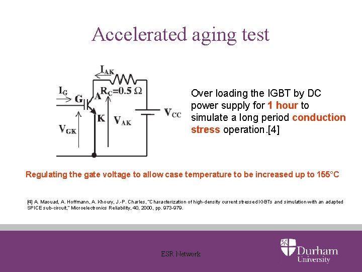
Accelerated aging test Over loading the IGBT by DC power supply for 1 hour to simulate a long period conduction stress operation. [4] Regulating the gate voltage to allow case temperature to be increased up to 155°C [4] A. Maouad, A. Hoffmann, A. Khoury, J. -P. Charles, “Characterization of high-density current stressed IGBTs and simulation with an adapted SPICE sub-circuit, ” Microelectronics Reliability, 40, 2000, pp. 973 -979. ESR Network
![Accelerated aging test Accelerated power cycling test system 5 It normally takes 2 3 Accelerated aging test Accelerated power cycling test system [5] It normally takes 2 -3](https://slidetodoc.com/presentation_image_h2/b1f5930d5c79d3161b0a8bb84e56489e/image-28.jpg)
Accelerated aging test Accelerated power cycling test system [5] It normally takes 2 -3 months to complete an aging test of approx. 600, 000 cycles [5] Xiong Y. , Cheng X. , Shen Z. J. , Mi C. , Wu H. , Garg V. , “A Prognostic and Warning System for Power Electronic Modules in Electric, Hybrid, and Fuel Cell Vehicles”, IEEE Industry Applications Conference, Oct. 2006, pp. 1578 – 1584. ESR Network

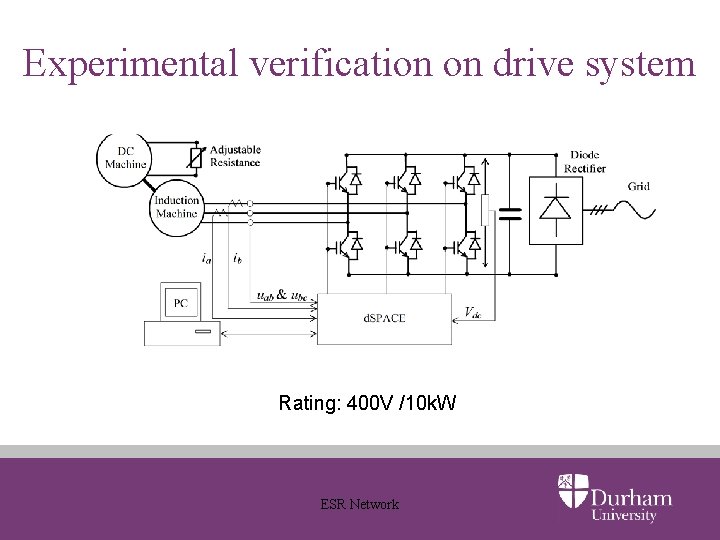
Experimental verification on drive system Rating: 400 V /10 k. W ESR Network

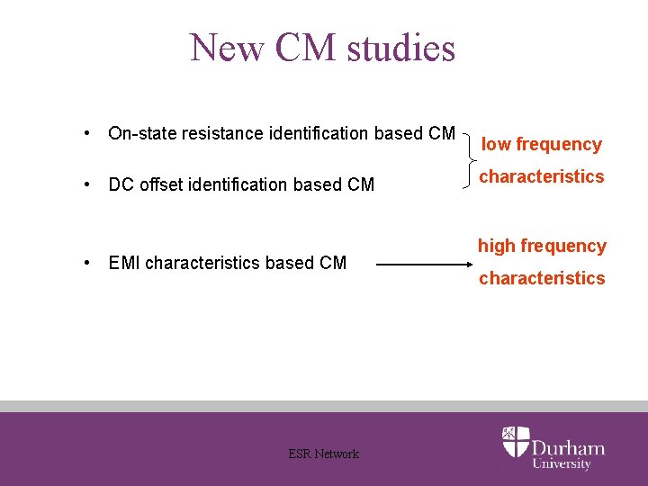
New CM studies • On-state resistance identification based CM • DC offset identification based CM • EMI characteristics based CM ESR Network low frequency characteristics high frequency characteristics

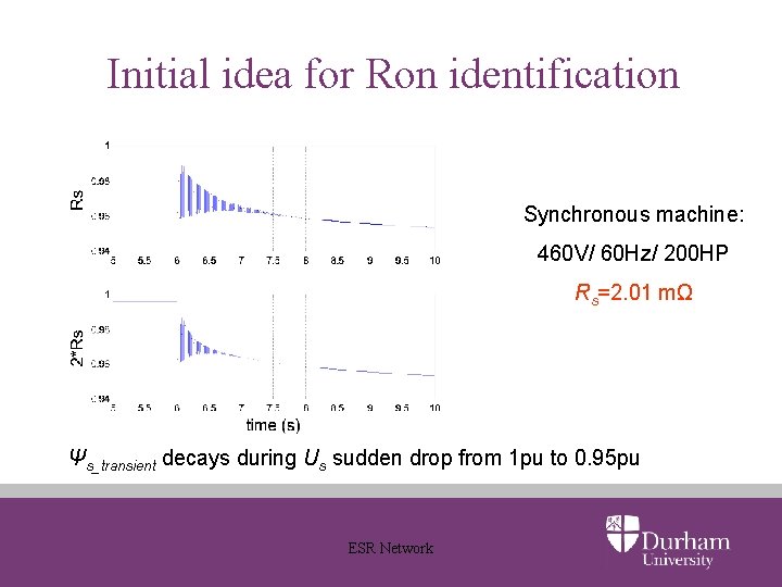
Initial idea for Ron identification Synchronous machine: 460 V/ 60 Hz/ 200 HP Rs=2. 01 mΩ Ψs_transient decays during Us sudden drop from 1 pu to 0. 95 pu ESR Network

Thanks for you attention! 32