COE 1502 Design Synthesis Synthesis Theory l Idea
- Slides: 14

COE 1502 Design Synthesis

Synthesis Theory l Idea: – “Compile” VHDL into a cell-level netlist l A netlist is a graph – Vertices represent cells (such as gates, latches, etc. ) – Edges represent interconnection wires l To do this, we need – VHDL – A technology cell library – Place-and-route netlist onto FPGA/ASIC l To do this, we need – Netlist – CLB specification and routing matrix (FPGA) l Output is FPGA routing bitmap

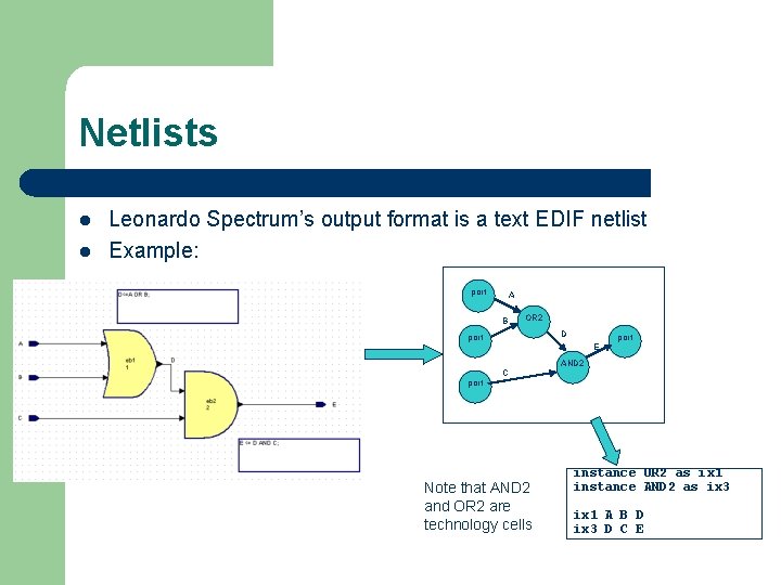
Netlists l l Leonardo Spectrum’s output format is a text EDIF netlist Example: port A B OR 2 D port E AND 2 port C Note that AND 2 and OR 2 are technology cells instance OR 2 as ix 1 instance AND 2 as ix 3 ix 1 A B D ix 3 D C E

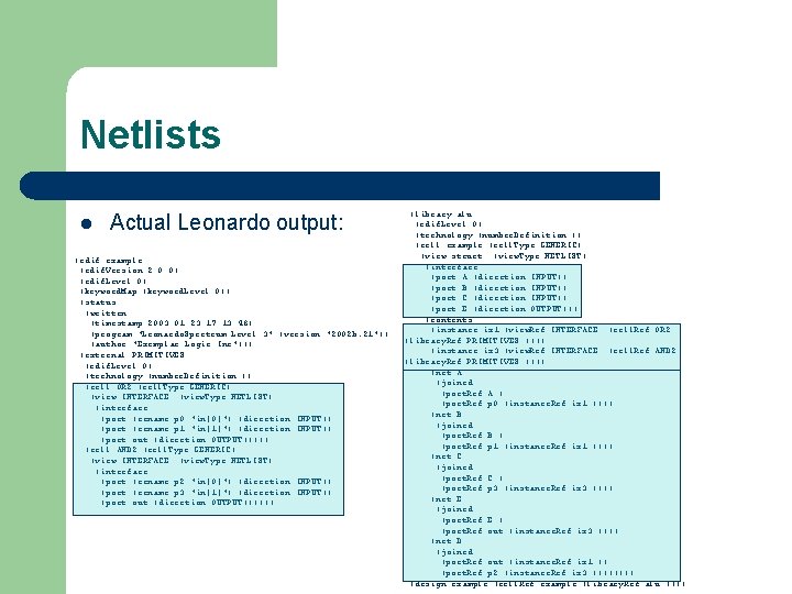
Netlists l Actual Leonardo output: (edif example (edif. Version 2 0 0) (edif. Level 0) (keyword. Map (keyword. Level 0)) (status (written (timestamp 2003 01 23 17 13 48) (program "Leonardo. Spectrum Level 3" (version "2002 b. 21")) (author "Exemplar Logic Inc"))) (external PRIMITIVES (edif. Level 0) (technology (number. Definition )) (cell OR 2 (cell. Type GENERIC) (view INTERFACE (view. Type NETLIST) (interface (port (rename p 0 "in[0]") (direction INPUT)) (port (rename p 1 "in[1]") (direction INPUT)) (port out (direction OUTPUT))))) (cell AND 2 (cell. Type GENERIC) (view INTERFACE (view. Type NETLIST) (interface (port (rename p 2 "in[0]") (direction INPUT)) (port (rename p 3 "in[1]") (direction INPUT)) (port out (direction OUTPUT)))))) (library alu (edif. Level 0) (technology (number. Definition )) (cell example (cell. Type GENERIC) (view struct (view. Type NETLIST) (interface (port A (direction INPUT)) (port B (direction INPUT)) (port C (direction INPUT)) (port E (direction OUTPUT))) (contents (instance ix 1 (view. Ref INTERFACE (cell. Ref OR 2 (library. Ref PRIMITIVES )))) (instance ix 3 (view. Ref INTERFACE (cell. Ref AND 2 (library. Ref PRIMITIVES )))) (net A (joined (port. Ref A ) (port. Ref p 0 (instance. Ref ix 1 )))) (net B (joined (port. Ref B ) (port. Ref p 1 (instance. Ref ix 1 )))) (net C (joined (port. Ref C ) (port. Ref p 3 (instance. Ref ix 3 )))) (net E (joined (port. Ref E ) (port. Ref out (instance. Ref ix 3 )))) (net D (joined (port. Ref out (instance. Ref ix 1 )) (port. Ref p 2 (instance. Ref ix 3 )))) (design example (cell. Ref example (library. Ref alu ))))

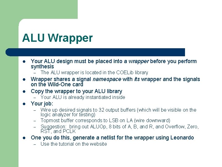
ALU Wrapper l Your ALU design must be placed into a wrapper before you perform synthesis – l l Wrapper shares a signal namespace with its wrapper and the signals on the Wild-One card Copy the wrapper to your ALU library – l Your ALU is already instantiated inside Your job: – – – l The ALU wrapper is located in the COELib library Wire up desired signals to 32 output buffers (which will be visible on the logic analyzer for testing) Topmost buffer corresponds to LSB on LA (wire downward) Suggestion: bring out ALUOp, 8 bits of A, B, and R, and Overflow, Zero, RST, and PCLK One you do this, generate a netlist for the wrapper using Leonardo – Use the tutorial on the website

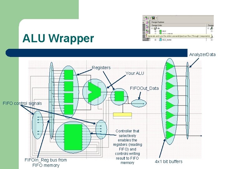
ALU Wrapper Analyzer. Data Registers Your ALU FIFOOut_Data FIFO control signals FIFOIn_Reg bus from FIFO memory Controller that selectively enables the registers (reading FIFO) and controls writing result to FIFO memory 4 x 1 bit buffers

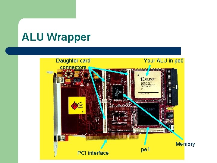
ALU Wrapper Daughter card connectors PCI interface Your ALU in pe 0 pe 1 Memory

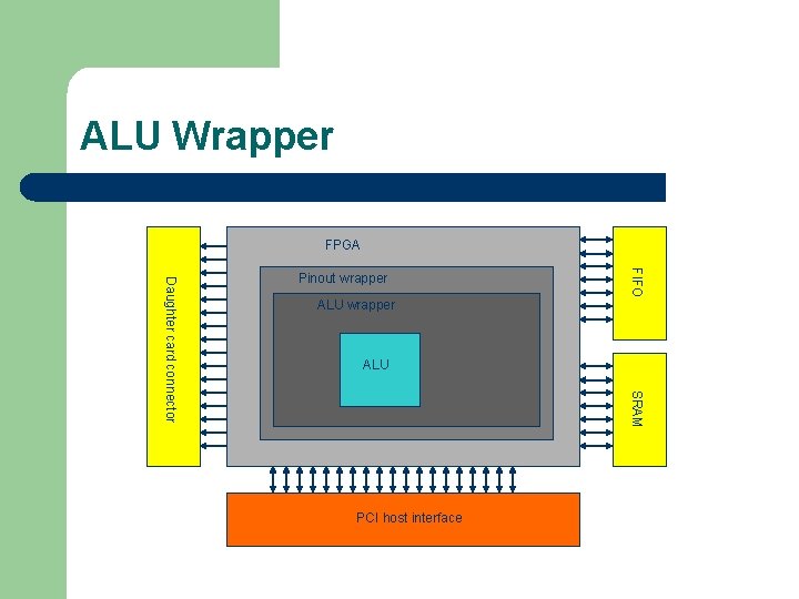
ALU Wrapper FPGA ALU wrapper FIFO ALU SRAM Daughter card connector Pinout wrapper PCI host interface

Preparing for Synthesis l Copy the CPE 0 directory from I: 1502 to your group directory… – This is the directory where you will perform synthesis, place-and-route, and test your design using the logic analyser

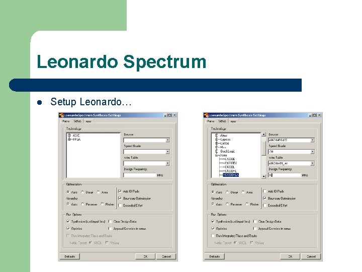
Leonardo Spectrum l Setup Leonardo…

Leonardo Spectrum l If the synthesis completes without error, copy ALU_WRAP. edf from <ALU_root>lsnetlistsalu_wrap_structnetlistsalu_wrap. edf into your CPE 0 directory.

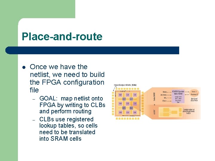
Place-and-route l Once we have the netlist, we need to build the FPGA configuration file – – GOAL: map netlist onto FPGA by writing to CLBs and perform routing CLBs use registered lookup tables, so cells need to be translated into SRAM cells

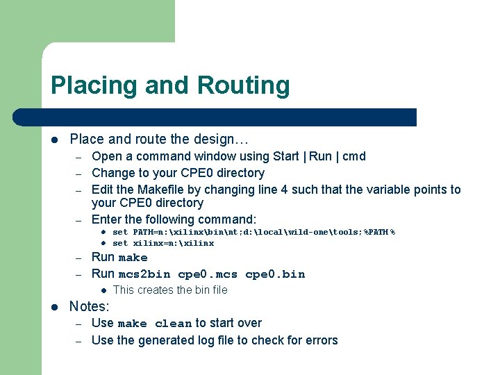
Placing and Routing l Place and route the design… – – Open a command window using Start | Run | cmd Change to your CPE 0 directory Edit the Makefile by changing line 4 such that the variable points to your CPE 0 directory Enter the following command: l l – – Run make Run mcs 2 bin cpe 0. mcs cpe 0. bin l l set PATH=n: xilinxbinnt; d: localwild-onetools; %PATH % set xilinx=n: xilinx This creates the bin file Notes: – – Use make clean to start over Use the generated log file to check for errors

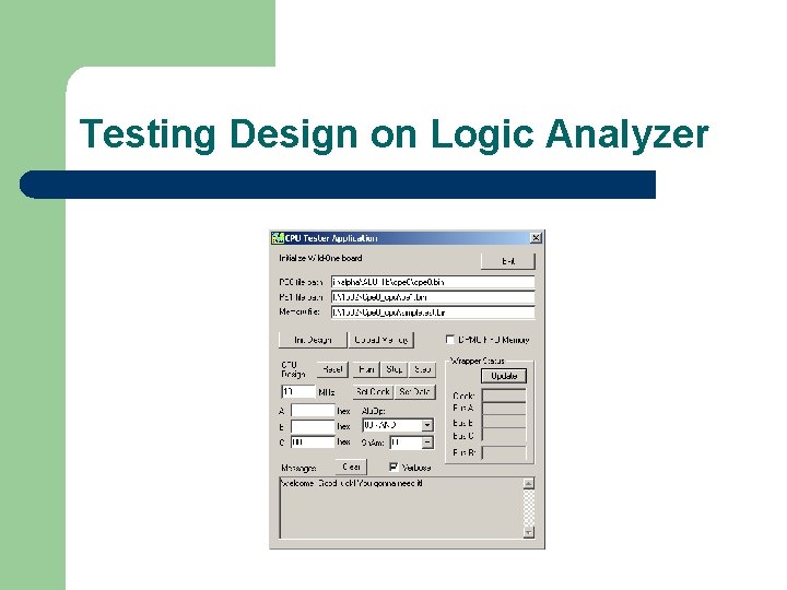
Testing Design on Logic Analyzer